
Oxide TFT stability and contact resistance, both held by a laser
A study with Samsung Electronics' Semiconductor R&D Center as a joint participant. A single process step, one pass of a laser over the tungsten gate, captured both oxide TFT stability (PBS threshold voltage shift down 83%) and contact resistance (down 59%), while the data retention of a capacitor-less DRAM cell jumped from 34.8% to 87.9%. A result to collect for any team looking for next-generation process candidates.
DOI 10.1002/adfm.77445Using an oxide TFT as a memory device means satisfying two conflicting conditions at once: a positive threshold voltage to hold the cell state stably, and a current large enough to read quickly. A DGIST and Samsung Electronics team captured both merely by passing a laser once over the metal gate. The threshold voltage shift fell 83%, and data retention jumped from 34.8% to 87.9%.
1. Why this was a hard problem
Building the read transistor as a dual-gate structure requires a stable positive threshold voltage for the cell to compensate its own state, and a large drive current (above 3µA) for fast read operation. But the two eat into each other. Removing defects such as oxygen vacancies to obtain a positive threshold voltage reduces the channel’s carrier density, and lower carrier density brings mobility down with it (the percolation conduction mechanism). On top of that the contact characteristics at source and drain worsen, making charge injection harder, so the drive current loses twice over.
The methods tried so far each had their price. Chemical treatments (hydrogen plasma, fluorine doping) risked damaging the device, and structural designs such as heterojunction contacts complicated the process. Ordinary furnace annealing takes long enough for impurities to leak in from the surrounding layers, and ultraviolet laser annealing instead increased oxygen vacancies, pushing the threshold voltage negative and damaging the channel. A method satisfying both conditions at once without damage and without adding process steps remained unsolved homework.
2. The turn: a laser that heats only the metal gate
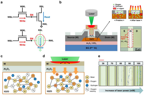
The group applied a 532nm continuous-wave (CW) laser selectively to the tungsten (W) top gate electrode rather than the whole device. As the tungsten absorbs the laser, a steep thermal gradient forms in the vertical direction, and that single gradient does two things at once.
- Oxygen redistributes toward the interface between the gate dielectric (Al₂O₃) and the IGZO channel, reducing oxygen vacancy and hydroxyl defects. The threshold voltage moves positive, and since the bulk carriers are not greatly lost, mobility is maintained
- At the same time the resistive tungsten oxide (WOx) interfacial layer at the source and drain contacts decomposes, creating conductive n+ regions. Contact resistance falls
Optimizing channel and contacts at once with a single laser exposure, with no separate chemical treatment or structural change, is the core of this work.
3. Result: both the transistor and the memory cell improved
Table 1 · Before and after laser annealing (70mW)
| Metric | Before laser | After laser | Measurement condition |
|---|---|---|---|
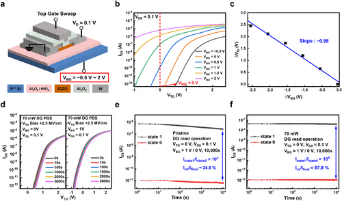
| mobility | not reported | 37.9 cm²/V·s | dual-gate operation, VDS=0.1V |
| threshold voltage | negative | +0.27 V | dual-gate operation, VDS=0.1V |
| on/off current ratio | not reported | >10⁹ | VDS=1V |
| PBS threshold voltage shift (3600 seconds) | 738 mV | 122 mV | +2.5 MV/cm applied |
| contact resistance | 15.9 Ω·cm | 6.5 Ω·cm | TLM measurement |
| Schottky barrier (W/IGZO) | 0.77 eV | 0.52 eV | from UPS and UV-vis |
Laser power is effective only in the 30 to 70mW range; thermal damage occurred above 80mW. Source: paper Table 1, Figures 4 and 6.
Putting the laser-treated device in as the read transistor of a 2T0C (two transistors, zero capacitors) DRAM cell, the memory window was maintained above 10⁵ and the inter-gate coupling slope recorded -0.98V/V, close to the theoretical limit (-1V/V). The most striking part is the retention test. Under repeated read operations for 10,000 seconds, the device before laser treatment saw its “1” state current fall to 34.8% of its initial value, while the laser-treated device held 87.9%.
4. What it means: one step that can be added to backplane process
IGZO TFTs are already the core material of display backplanes, and the capacitor-less DRAM this result targets points toward widening that application range into memory. That it exposes only the gate metal selectively, with existing laser annealing equipment and no separate chemical process or structural change, suggests it could be laid onto a large-area panel process line without an additional process burden.
This validation is at individual device scale, though, and interference or yield when many cells operate together in a real high-density array has not yet been addressed. The retention test also went only as far as 10,000 seconds (about 2.8 hours).
5. At a glance
| In one line | selective laser exposure of the tungsten gate improves IGZO TFT stability (ΔVth down 83%) and contact resistance (down 59%) at once |
| Core results | mobility 37.9cm²/V·s · PBS ΔVth 122mV (down 83%) · contact resistance 6.5Ω·cm (down 59%) · DRAM retention 87.9% |
| Strengths | channel and contacts optimized together by a single laser exposure, with no chemical treatment or structural change |
| Published | Advanced Functional Materials, 2026 (Early View) |
6. Key terms
- dual-gate (DG) TFT
- A transistor structure with two gates, top and bottom. Writing data with one gate and reading with the other lets it work like a memory cell without a capacitor.
- 2T0C DRAM
- A DRAM cell structure built from two transistors and using no capacitor. One of the next-generation memory candidates bypassing the physical limits of capacitor miniaturization.
- PBS / threshold voltage (Vth)
- PBS (positive bias stress) is a standard stability test stressing the device by holding a positive voltage on the gate. The threshold voltage is the voltage at which the transistor starts to turn on, and how far it drifts during the test is the stability indicator.
- Schottky barrier
- The energy barrier formed where a metal joins a semiconductor. The lower it is, the more easily charge crosses and the lower the contact resistance.
The other 9 papers of the week (and one in-depth article on the flexible OTFT) are swept briefly in the display paper briefing for week 4 of July.