Twelve nano LED patents analysed
There are two ways to put a nano LED onto a screen. Make it separately and lay it down, or grow it standing up in place. The two opposite methods both came out of university laboratories, and in both lineages the patents ended up at Samsung. One whole day, 7 September 2018, sits in the US Patent Office assignment records. And yet the company now building a mass production line is France's Aledia, which did not sell its patents.
This article was published before the English edition began, so the labels inside its figures and simulators are in Korean. The caption and the note under each figure are in English.
1. Overview
1.1 Background and purpose
There are broadly two ways of putting nanometre-scale light-emitting diodes onto a screen. One makes the LEDs separately on a wafer, floats them in a liquid, sprays them onto a substrate and lays them down with an electric field; the other grows them vertically in place on the substrate. The former is what Samsung Display has developed under the name QNED, the latter what France’s Aledia has taken into a mass production line for augmented reality microdisplays.
The two methods are physically opposite. And yet following the bibliographic records of the granted patents turns up one thing in common. Both lineages started at universities and national laboratories, and the patents of both lineages ended up at Samsung. One was bought by Samsung Display, the other by Samsung Electronics. And the company now building a line and making product is the one that did not sell.
This piece confirms that configuration through bibliographic records and claims, and works out why laying them down is hard, using the numbers written into the claims.
1.2 Scope
12 granted patents were taken as the sample: 8 on the laying-down side, 3 on the growing-up side, and 1 as a contrast case. It is not an exhaustive survey but a sample of landmarks chosen from each camp, selected on the pipeline’s five indicators (number of family countries, grant status, abandonment or lapse, divisional and continuation offspring, same-day filing clusters) and on the assignment history that is this piece’s axis.
Two things were deliberately left out. One is micro LED mass transfer. Once device size rises above single-digit micrometres, both the forces handled and the process change, and putting it in the same piece blurs the focus. The other is QNED’s colour conversion layer (quantum dots). This piece’s axis is the problem of seating a device in its place, not the problem of changing its colour once seated.
1.3 Data source and search strings
| Search string | Publications | Granted |
|---|---|---|
"dielectrophoresis" + assignee=Samsung Display | 345 | 154 |
"nanorod" + assignee=Samsung Display | 522 | 168 |
| assignee=Aledia | 713 | 193 |
| assignee=Glo AB | 90 | 71 |
"self-assembly" "light emitting" + assignee=LG Electronics | 269 | 121 |
"dielectrophoresis" + assignee=BOE Technology | 15 | not checked |
"dielectrophoresis" + assignee=Shenzhen China Star Optoelectronics | 0 | 0 |
inventor=Young Rag Do + assignee=Samsung Display + US + priority from 2011 | 25 | 23 |
Google Patents, single source. The Korean register (KIPRIS) could not be obtained. That difference becomes a problem once later: transfers of rights on Korean grants do not appear in Google Patents bibliographic records. Every assignment confirmed in this piece is from the US Patent Office record on a US grant.
The numbers are all publication counts. The same invention published in Korea, the United States and China counts as three. They are not family-level counts, so they are not used to compare companies, only to look at distribution over time within one company.
1.4 Technical classification
This piece reads the patents on two axes. What is changed (the lever) is device structure, ink and solvent, electric field conditions, equipment and inspection, and substrate growth. What is being removed (the aim) is dispersion and injection, angle, polarity, count and yield, and colour.
Why the aim axis is drawn that way emerges in Sections 3 and 4. Spraying with ink and seating carries three different kinds of randomness, and the twelve sets of claims attack each of the three by different means.
2. Quantitative sketch
2.1 The two lineages on a timeline
The horizontal axis is priority date. The upper line is the laying-down side, the middle the growing-up side, the dashed line below the contrast case.
Three places are worth reading. First, the two lineages start only one year and five months apart. Kookmin University and PSI filed in April 2011, Aledia and the French Alternative Energies and Atomic Energy Commission (CEA) in September 2012. Second, the red vertical line is 7 September 2018. Third, immediately to the right of that line sit two of Samsung Display’s own filings. We come back to them.
2.2 What happened on 7 September 2018
US Patent Office assignment records are exposed directly in Google Patents’ legal events field. Open that field one by one for the US grants in the sample and the same date repeats.
| Patent | Original applicant | Assigned | Current owner |
|---|---|---|---|
| US9059114B2 | PSI Co Ltd | 2018-09-07 | Samsung Display Co Ltd |
| US9112112B2 | PSI Co Ltd | 2018-09-07 | Samsung Display Co Ltd |
| US9773761B2 | PSI Co Ltd | 2018-09-07 | Samsung Display Co Ltd |
| US9570425B2 | PSI Co Ltd | 2018-09-07 | Samsung Display Co Ltd |
| US9978725B2 | PSI Co Ltd | 2018-09-07 | Samsung Display Co Ltd |
| US10062804B2 | PSI Co Ltd | 2018-09-07 | Samsung Display Co Ltd |
| US10145518B2 | PSI Co Ltd | 2018-09-07 | Samsung Display Co Ltd |
| US9935241B2 | PSI Co Ltd | 2018-09-07 | Samsung Display Co Ltd |
| US10784246B2 | PSI Co Ltd | 2018-09-07 | Samsung Display Co Ltd |
| US11063194B2 | Samsung Display Co Ltd | not applicable | Samsung Display Co Ltd |
These were not picked at random; they are the first ten results opened from a search on this condition, and nine of them carry the same date. The remaining one is a continuation filed after the assignment, so it has no assignment event of its own.
Open US9112112B2 alone and the path the right travelled remains in four steps.
2014-01-24 inventors Young Rag Do and Yeon Goog Sung to PSI and Kookmin University Industry-Academic Cooperation Foundation
2014-07-24 Kookmin University Industry-Academic Cooperation Foundation to PSI
2015-07-13 share settlement
2018-09-07 PSI to Samsung Display
From inventors to joint holding by university and company, then to the company alone, and finally to a large corporation: four steps sitting in the public record.
inventor=Young Rag Do with assignee=Samsung Display and US returns exactly 40. It looked cross-verified, but opening the list showed fifteen cathode ray tube phosphor and organic light emitting patents from the Samsung Display Devices and Samsung SDI era, between 1994 and 2004. Same inventor, nothing to do with this lineage. Cut priority to 2011 and later and it is 25 (23 granted). This piece does not claim to have verified the reported figure.2.3 Where the twelve sit
An empty cell does not mean that company does not do it; it means it is not in this sample. Of the twelve, the LG Electronics contrast case is not placed in this grid. Its lever is magnetic force, a different axis.
What is visible at a glance is the bottom row. The laying-down side attacks dispersion, angle, polarity and count spread across four cells, while the growing-up side erases the left three as one block. Set the place a wire will grow by the arrangement of materials on the substrate surface and position, angle and polarity are not random to begin with.
2.4 How much Samsung Display has banked on this method
| Priority | 2017 | 2018 | 2019 | 2020 | 2021 | 2022 | 2023 | 2024 | 2025 |
|---|---|---|---|---|---|---|---|---|---|
| Publications | 1 | 35 | 53 | 43 | 20 | 81 | 21 | 8 | 0 |
This table is not interpreted here, for two reasons.
First, the collapse in 2024 and 2025 may not be a decline. An application is published only 18 months after its priority date. At the time of this survey most filings with a 2025 priority were not yet published.
Second, several reports say this development has been halted, but that could not be confirmed from primary material such as a disclosure or the company’s own announcement, and in the sample the 2022 priority year is the largest at 81. Reports and sample disagree, so no conclusion is drawn either way.
A third thing to add is a limit of the search string itself. The 345 caught by "dielectrophoresis" include cases unrelated to nanorod alignment. In fact US11170688B2 was put on the candidate list while building this sample and then removed after reading the claims. It was a method of driving an organic light emitting device containing a dielectrophoretic material in voltage ranges, not a technology for laying nanorods down.
3. Qualitative analysis: 12 patents
Arranged by priority date. The gist of claim 1, the problem the specification states directly and the numeric limitations are carried over from the original.
Title
Subminiature LED element and manufacturing method thereof
Gist of independent claim 1
A manufacturing method in which (a) a first conductivity type semiconductor layer, an active layer and a second conductivity type semiconductor layer are formed in order on a substrate, (b) these are etched so the LED element has a diameter at the nanometre or micrometre scale, and (c) an insulating film is formed on its outer circumference and the top of the insulating film is coated with a hydrophobic film, after which the substrate is removed.
The problem this patent addresses
Floating a device in a liquid and spraying it requires two things at once. The sides must be electrically insulated so there is no short when they touch an electrode, and the surface must get along with the liquid so it disperses rather than clumping. Claim 1 solves both with two layers, insulating and hydrophobic. The method of setting the diameter using nanospheres as a mask is written alongside in the specification.
Numeric limitations
Title
Full-color LED display device and manufacturing method thereof
Gist of independent claim 1
A manufacturing method forming a plurality of first electrodes on a substrate, attaching at least five subminiature blue LED elements at each unit pixel site formed on the first electrode, forming an insulating layer and a second electrode, then patterning a green colour conversion layer and a red colour conversion layer in turn at selected unit pixel sites.
The problem this patent addresses
The structure of making all three colours from one blue nanorod while changing colour with a conversion layer was already in the claims in 2011. It is the prototype of what is now called QNED.
But the number this piece will keep following is here. At least five per pixel. We meet this number again in Section 4.
Numeric limitations
Title
Optoelectric device with semiconductor microwires or nanowires and method for manufacturing the same
Gist of independent claim 1
A device having microwires or nanowires mainly comprising III-V compounds on a support, where the support surface is divided into first regions promoting growth by the polarity of a first element and second regions promoting growth by the polarity of a second element, and the wires are located on those first regions.
The problem the specification states
Making vertical sidewall structures of III-V compounds "at low cost on an industrial scale."
The problem this patent addresses
The core is the “first region” in the claim. Lay two different materials in a pattern on the substrate surface and wires grow only at the prescribed places. Position is decided by the mask, not at random. The problem the laying-down side wrestles with through ink concentration and electric field turns into a lithography problem here.
Numeric limitations
Title
Nano-scale LED element for horizontally-aligned assembly
Gist of independent claim 1
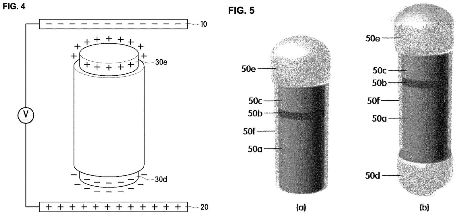
An LED element comprising first and second semiconductor layers with an active layer between them, an insulating film covering at least the outer circumference of the active layer, and an electrode placed directly on at least one of the semiconductor layers and contacting the top and part of the side of the insulating film. Dependent claim 3 limits its cross-section to a swab shape or a dumbbell shape.
The problem this patent addresses
To lay a rod across two electrodes, both ends have to touch the electrodes while the sides must not. So the sides are covered with an insulating film and metal caps go on the ends alone. The cross-section then comes to resemble a cotton swab or a dumbbell. The right-hand side of the figure below is that shape.
The specification contains a sentence declining to specify the alignment voltage and frequency, stating that the conditions depend on the aspect ratio of the device.
Numeric limitations
Title
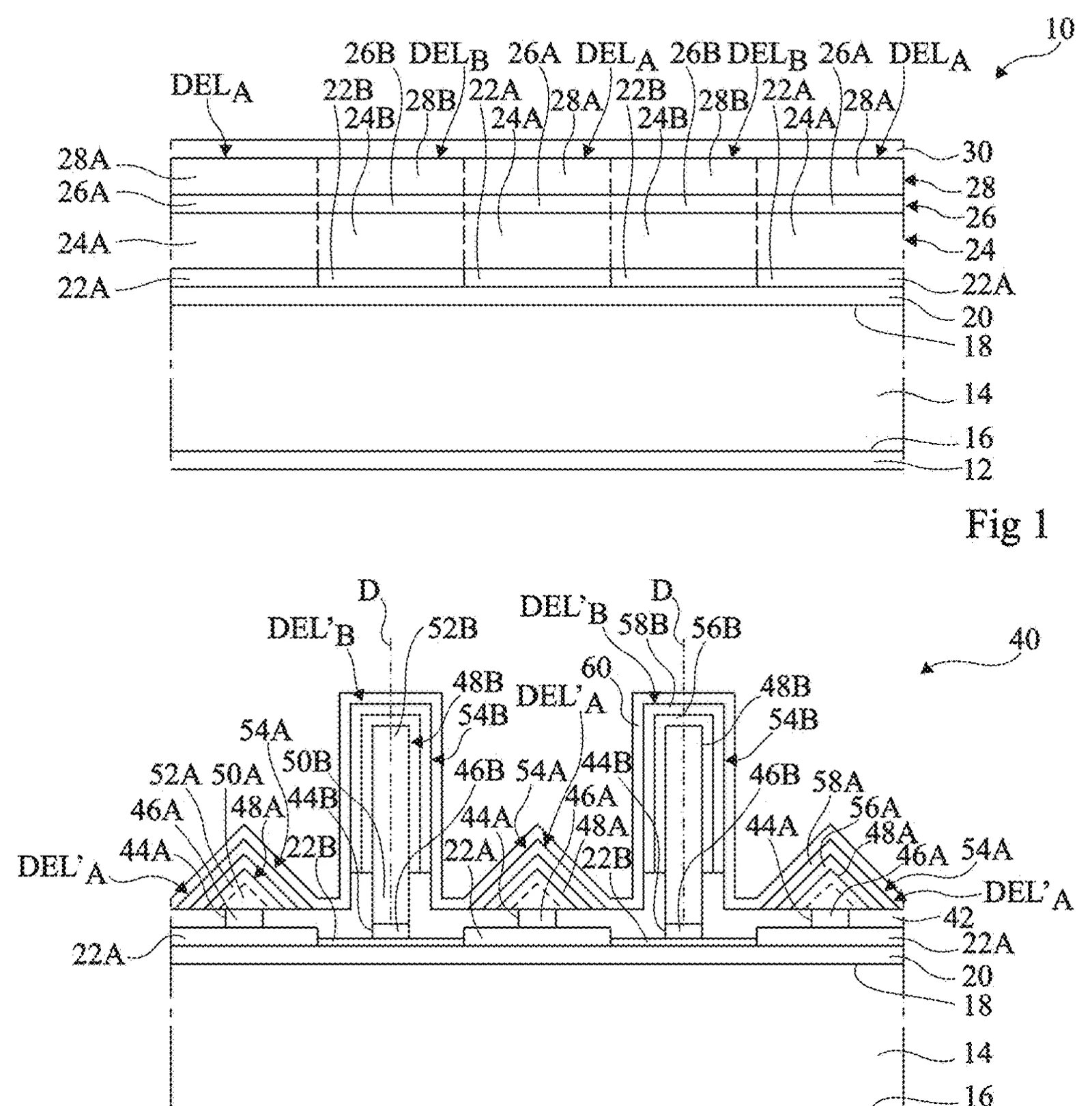
Optoelectronic device comprising three-dimensional electroluminescent diodes
Gist of independent claim 1
An optoelectronic device placing on a substrate a pyramid-shaped semiconductor portion of a first polarity together with a semiconductor portion of a different second polarity, with first and second active regions mainly comprising III-V or II-VI compounds each in contact with them.
The problem this patent addresses
Pyramids and wires are stood on the same substrate together. The specification states that when the cross-sectional diameter and the slope differ, the amount of indium incorporated differs and so does the emission wavelength. That is, colour is separated by shape alone under the same growth conditions.
The laying-down side has to make a different device for each colour and spray them separately, or make one blue and lay a colour conversion layer on top. This patent pushes that process into the growth step.
Numeric limitations
Title
Nano-scale LED electrode assembly emitting polarized light
Gist of independent claim 1
An electrode assembly comprising first and second mounting electrodes separated in the same plane, and a plurality of nano-scale LED elements with one lengthwise end contacting the first electrode and the other the second, wherein the number of elements having a mounting angle within ±30 degrees of the average mounting angle of all emitting elements is above a certain proportion.
The problem this patent addresses
This claim takes the scatter of the alignment itself as the scope of the right. It presupposes that the rods do not all lie in the same direction, and defines quality by the proportion falling within ±30 degrees of the average. The resulting polarization ratio is limited by a formula.
The specification names an earlier granted patent (KR 10-1490758) directly, stating that “the nano-scale LED elements are not aligned as desired.” It designates a preceding patent within its own lineage as the problem.
Numeric limitations
Title
Solvent for manufacture of self-assembled nano-scale LED electrode assembly
Gist of independent claim 1
A manufacturing method feeding nano-scale LED elements and a solvent onto electrode lines and applying power to self-align them, wherein the solvent evaporates simultaneously with or immediately after the alignment step.
The problem this patent addresses
The solvent itself being the subject of the invention makes this the only such case in the sample. The specification demands four conditions, stating that low viscosity keeps the devices from spreading well while high viscosity worsens the alignment. Boiling point and vapour pressure come from the requirement that the solvent fly off the moment alignment is finished. A solvent that dries late lets seated devices move again.
Numeric limitations
Title
Ultra-small LED electrode assembly having improved luminance
Gist of independent claim 1
A manufacturing method feeding a solution containing a plurality of LED elements onto electrode lines and applying power with an asymmetric assembly voltage of 10V or more according to formula 1 to self-mount the elements, with at least one end of each element contacting the first electrode.
The problem this patent addresses
This is the most important claim in the piece. The specification states that at least 60% of the elements must have their first conductivity type semiconductor touching the first electrode.
An electric field lays the rod down but cannot decide which end touches which electrode. With a symmetric waveform half lie the wrong way, and under DC drive that half does not light. So an asymmetric waveform, different above and below, is applied to raise the proportion in one direction. Even then 40 percent are reversed.
The specification also gives its own reason for the frequency floor. Below 50kHz, it says, the number of devices mounted falls even when the voltage range is satisfied. The statement is that the count drops, not that the angle scatters. Section 4.2 follows this sentence with a calculation.
Numeric limitations
Title
Apparatus and method for self-assembling of semiconductor light-emitting diodes
Gist of independent claim 1
A self-assembly apparatus comprising a fluid chamber holding semiconductor light-emitting devices having a magnetic body, a supply carrying the substrate to the assembly position, a plurality of magnets arranged away from the chamber applying magnetic force to the light-emitting devices, and a position controller controlling the magnets' positions, wherein the substrate forms an electric field so the light-emitting devices are mounted at prescribed positions.
The problem this patent addresses
LG’s method is commonly called self-assembly, but reading the claim, magnetic force and electric field are used separately. The magnets handle transport, dragging devices through the fluid, while the electric field the substrate makes finally seats them. The specification also describes recovering leftover devices from the chamber with a magnet for reuse.
The devices this method handles, though, are micro rather than nano scale. This is the only case in the sample in a different size band, which is why it was not placed in the grid.
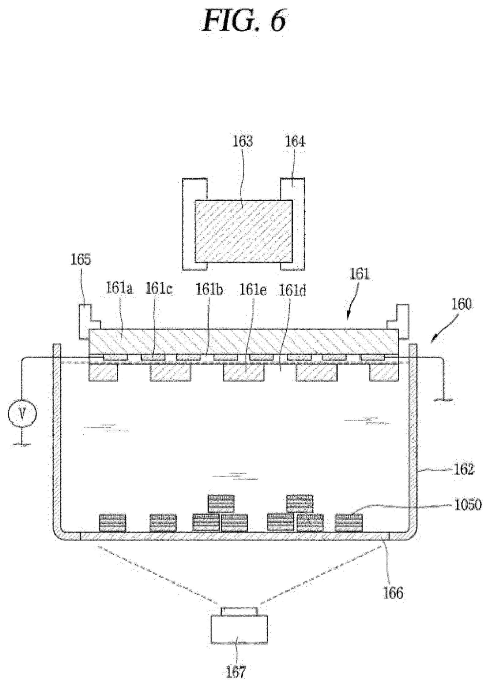
Title
Inkjet printing apparatus, dipole alignment method, and display device manufacturing method
Gist of independent claim 1
An inkjet printing apparatus comprising a stage, a print head unit above it, and an electric field generator including an antenna unit and providing a horizontal electric field parallel to the principal surface of the stage in the space between stage and print head.
The problem this patent addresses
The idea moves a step earlier. The established method drops the ink onto the substrate and then aligns with the substrate’s electrodes. This patent sets the direction already in the space between head and stage, in mid-air while the ink is falling. Two or more antennas make a horizontal electric field in that space.
The priority date is 21 September 2018. Two weeks after the assignment of 7 September.
Numeric limitations
Title
Inkjet printing device, dipole aligning method, and display device
Gist of independent claim 1
An inkjet printing apparatus comprising a stage unit, an inkjet head unit placing ink containing dipoles and a solvent on the stage, a heat treatment device removing the solvent, a first sensing unit measuring the position of the ink, a second sensing unit measuring the position of the head, and a third sensing unit measuring the position of each individual dipole placed on the stage.
The problem this patent addresses
The claim contains three sensing units, and the third is this piece’s concern. Not the position of the ink droplet, nor the position of the head, but the position of each individual dipole, that is, each nanorod.
An item like this entering an equipment claim reads as meaning the alignment result had to be counted device by device. This is an inference from the claim’s composition, though, and how it is actually operated on a production line cannot be confirmed.
Numeric limitations
Title
Subpixel light emitting diodes for direct view display and methods of fabricating the same
Gist of independent claim 1
An LED transfer method placing a first substrate carrying LEDs emitting a first colour and a second substrate carrying LEDs emitting a second colour, transferring a subset of the first LEDs to bonding structures of a first backplane to form subpixels in a pixel area and separating them from the substrate, and transferring a subset of the second LEDs to a second backplane, leaving vacancies in the second substrate.
The problem this patent addresses
Even within the growth camp, the approach differs from Aledia’s. The specification states that the n-type semiconductor region is formed as a nanowire core, nanopyramid or nanofrustum, making its growth basis clear, while the claim covers transfer to a backplane after growth. It is a hybrid, made by growth and placed by transfer.
Because it leaves vacancies in the substrate and fills them with another colour, the aim reads as sharing a wafer across colours rather than discarding it.
Numeric limitations
4. Comparative analysis
4.1 The randomness is not one but three
The process of floating rods in a liquid, spraying them and seating them with an electric field carries three kinds of randomness, different in character. The twelve sets of claims attack these three by different means, and without separating them there is no explaining why so many patents are needed.
| What is random | The laying-down response | The growing-up side | |
|---|---|---|---|
| Position | how many land in each pixel | ink concentration and alignment time (US9059114, at least 5 per pixel) | the growth mask designates the site (US9245948) |
| Angle | how parallel they lie | field conditions, device shape (US10145518, ±30 degrees) | growth direction is the direction |
| Polarity | which end touches which electrode | asymmetric waveform (US10361246, 60% or more) | growth order decides it |
This table is the skeleton of the piece. The two sections below take angle, then polarity and count, in turn.
4.2 Angle was not the problem
Angle was calculated first. A simulator showing how the force laying a rod down by dielectrophoresis contends with thermal motion. The voltage and frequency ranges the patents claim are laid directly over the physical limits.
Three values can be read at the default.
First, the voltage at which the field ties with thermal motion is 0.011V. That is 1/5,000 of the 60V the patents use. Apply a field on the order of 10 to the 7th volts per metre to a rod 4μm long and the alignment energy becomes ten million times the thermal energy. Laying rods down parallel is not in itself hard. At this size Brownian motion is no contest.
Second, the upper wall is dielectric breakdown of the solvent. At an electrode gap of 3μm it is about 120V, and the patents’ upper limit of 100V (±50V) sits just below it.
Third, so the wall that actually remains is the one on the left. Push the frequency slider left and the double layer at the electrode surface screens the field, reducing what is applied inside the solution. In this model the stability line comes out at about 25kHz, and the 50kHz floor claimed by US10361246B2 lies above it while the 10kHz floor claimed by US11685154B2 lies below.
And what sets the position of this wall is the solvent. Raise the conductivity slider to 10 to the minus 2nd and the stability line rises to 252kHz, and half the claimed range disappears.
One caution here. The wall this model draws is an approximation based on double layer screening and AC electro-osmotic flow, while the 50kHz in the specification is an experimental value. The closeness of the two numbers is not read as evidence the model is right. That the specification’s stated reason for the floor was “the number of devices mounted falls” does not, however, run against this direction. When the field weakens, what scatters is not the angle but the number caught.
And if angle really was not the problem, why did US10145518B2 put ±30 degrees into its claim? Because the calculation deals only with thermal motion. The real scatter comes from elsewhere: fluid flow, rods already seated distorting the field for the next rod, non-uniform field at the electrode edges. What the calculation tells us is not “the alignment works well” but “the cause of the scatter is not thermal motion.”
4.3 What the electric field cannot decide
Even with the angle fixed, polarity remains. The force laying a rod down does not distinguish its two ends. The induced dipole aligns along the field direction, but turning that axis 180 degrees leaves the energy identical. So under a symmetric waveform, which electrode the p-type touches becomes a coin toss.
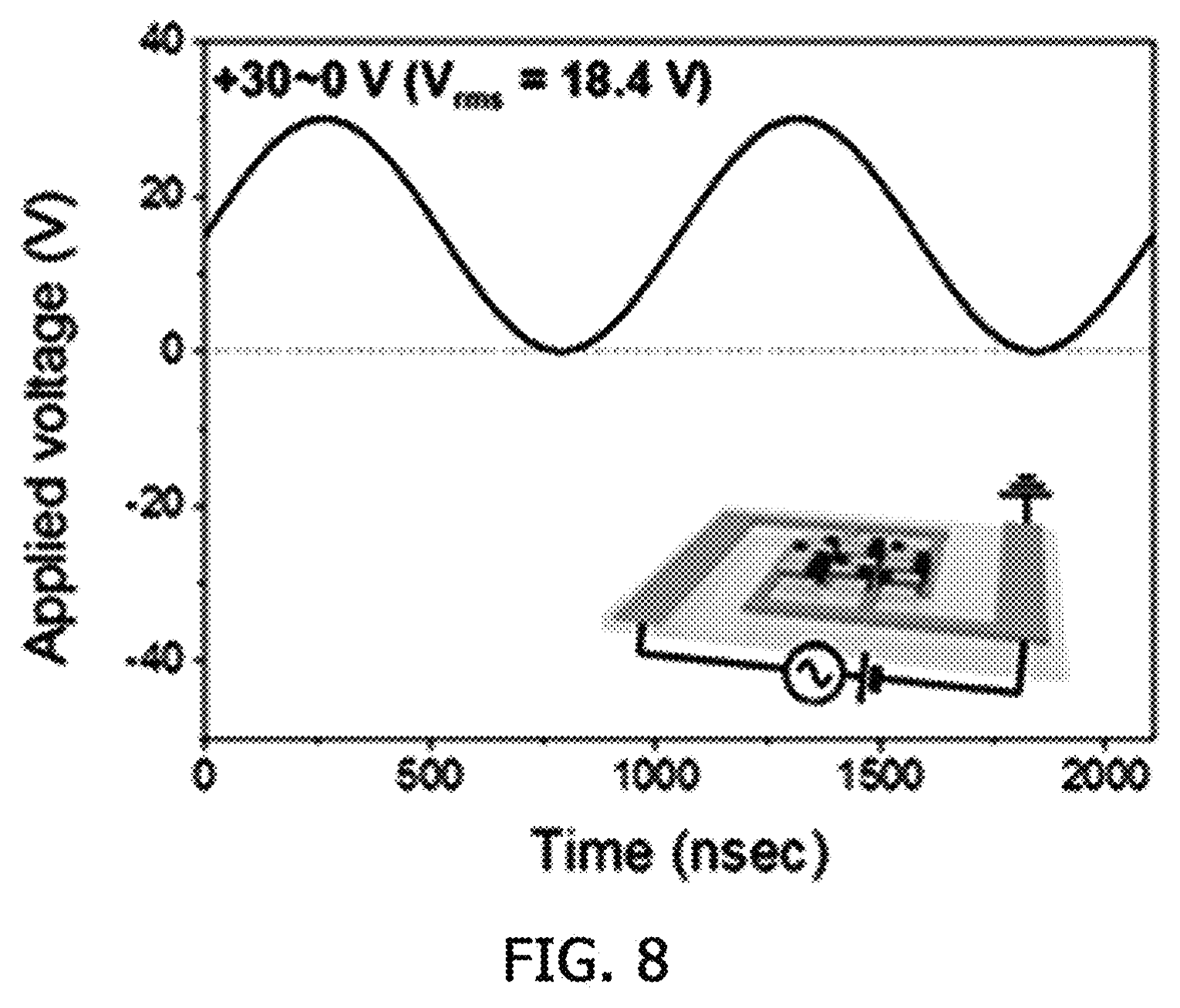
This is why US10361246B2 uses an asymmetric waveform. The waveform in the figure above does not go negative, swinging only between 0V and +30V. Its RMS value is 18.4V. Doing this creates a force biased in one direction, raising the matching proportion, and the point the specification records reaching is 60% or more.
Turn that around and the other 40% are lying the wrong way. Under DC drive that 40% does not light.
4.4 Count is luminance
Now to the randomness of position. Spray with ink and the number landing in each pixel scatters, and only those with matching polarity light. If pixel luminance is proportional to the number lit, that scatter becomes luminance scatter directly.
Assume a Poisson distribution with the sprayed count as its mean, and keeping only those with matching polarity leaves a Poisson distribution again. So the luminance coefficient of variation is inversely proportional to the square root of the number lit. The arithmetic becomes very simple.
Put the number from the original 2011 patent into it. What claim 1 of US9059114B2 demanded was at least five per pixel. Apply 60 percent polarity and the average number lighting is three, and the luminance coefficient of variation is 58 percent. Pixels differ in brightness by half.
Take 3 percent as the threshold at which mura becomes visible and the required count follows.
| Sprayed | Lit (60% polarity) | Luminance CV | Area share, 65-inch 4K subpixel | Area share, mobile subpixel |
|---|---|---|---|---|
| 5 | 3 | 57.7% | 0.03% | 1.0% |
| 100 | 60 | 12.9% | 0.5% | 20% |
| 1,000 | 600 | 4.1% | 5.1% | 200% |
| 1,852 | 1,111 | 3.0% | 9.5% | 370% |
Meeting 3 percent means spraying 1,852 per pixel. Taking one rod as occupying 4μm by 0.6μm, in a 65-inch 4K subpixel (short side 125μm) that is 9.5 percent of the area. It fits.
Put the same number into a mobile subpixel (short side 20μm) and it is 370 percent. It does not fit.
The smaller the pixel, the less room to raise the count, and without raising the count the scatter grows. That this method headed for television from the start can be read not as chance but as a matter of area.
This calculation is more optimistic than reality, though. Every rod was taken to be equally bright, and neither the effect of seated rods blocking the place of the next nor the positional correlation of crowding near the electrodes was included. The real scatter is larger.
4.5 Grow them up and three vanish at once
Return to claim 1 of US9245948B2. The support surface is divided into regions of two materials and wires grow only in one of them.
That single sentence erases three rows of the previous section’s table at once. Position is set by the mask, angle by the growth direction, polarity by the growth order. Lay n-type first, put the active layer on and cover with p-type, and there is no way for top and bottom to be reversed.
Other problems come instead. Lattice mismatch in growing gallium nitride on silicon, keeping wire height and diameter uniform across a whole wafer, and colour. US10424692B2 solves the last by shape. Under the same growth conditions, varying cross-sectional diameter and slope changes the amount of indium incorporated and hence the wavelength.
That the device dimensions of the two camps overlap is worth setting out. The rods the laying-down side handles and the wires the growing-up side makes are in almost the same size band. Physically the same-sized object, made and then moved by one, grown in place by the other.
4.6 7 September 2018, and two weeks later
Back to the timeline. Within the sample, the earliest priority date among Samsung Display’s own filings is US12004412B2, 21 September 2018. Two weeks after the assignment of 7 September.
That patent’s claim sits at a different layer from those before it. Where the PSI patents dealt with device, solvent and voltage conditions, this one claims equipment applying an electric field in mid-air while the ink is falling, setting the direction in advance. And four months later US11685154B2 puts a sensing unit measuring the position of individual dipoles into an equipment claim.
The axis moves from material and conditions to equipment and metrology. This observation rests on a sample of twelve, though, and does not say Samsung Display made no related filings before that.
4.7 The one that did not sell
Glo AB’s patent history holds something unlike either lineage above.
2021-08-13 assigned to Nanosys
2022-04-01 security interest granted with Fortress Credit Corp. as agent
2023-09-07 security released
2023-10-05 renamed Sysonan
current owner Samsung Electronics Co Ltd
Even the record of a security interest being granted and released remains. Nanowire LED patents out of Lund University in Sweden changed hands several times before reaching Samsung Electronics.
Over the same period Aledia holds 193 granted patents in its own name. Several also keep the French Alternative Energies and Atomic Energy Commission and the National Centre for Scientific Research as joint owners. Of three filed on a single day, 28 December 2012, FR3000613B1 lapsed for non-payment of annuities. It discards what it discards and holds the rest.
In sum, then. The patents out of Kookmin University went to Samsung Display, the patents out of Lund University to Samsung Electronics. The patents out of the French national laboratories were not sold. And the company that has announced a mass production line for nano LED is the one that did not sell.
This sentence is not causation. It does not mean that selling the patents is why mass production was not reached, nor the reverse. It is only the picture the bibliographic records draw.
4.8 After the assignment
It looks as though the story closes on 7 September 2018. It does not.
Nineteen months after the assignment, on 27 April 2020, “micro-nanofin LED element” was filed. The applicant is not PSI but the Kookmin University Industry-Academic Cooperation Foundation, and the inventor is Young Rag Do. According to reports it is the product of national research and development projects including a Ministry of Science and ICT research centre programme.
What deserves attention is not the claims but the background art in the specification.
To overcome such difficulties, granted patent publication No. 10-1436123 discloses a display manufactured by a method of dropping a solution containing nanorod-type LEDs onto a subpixel and then forming an electric field between two alignment electrodes to self-align the nanorod-type LED elements on the electrodes, thereby forming the subpixel. However, the nanorod-type LEDs used have a small light extraction area and thus poor efficiency, so that a large number of LEDs must be mounted in order to obtain the intended efficiency, and the nanorod-type LEDs themselves have a high likelihood of defects.
Where that No. 10-1436123 came from is set out in the same specification.
A detailed description of this is incorporated by reference from granted patent publications No. 10-1490758 and No. 10-1436123, by the inventor of the present invention.
The background art section is written by the applicant, and disclosing prior art is required by patent law. So this passage means it was not concealed, and no more than that. What is worth reading is elsewhere: what limit was named.
That obtaining the intended efficiency requires mounting a large number. This is where the simulator arrived in Section 4.4. How many land in a pixel sets the luminance scatter, and the route to raising the count is blocked by subpixel area. We put that calculation together belatedly by overlaying two claims; the inventor wrote it into a specification in one sentence in 2020. This method’s limit was documented from the inside before it was pointed out from the outside.
The nanofin is the answer to that sentence. Turn the rod into a plate and the light-emitting area for the same volume widens, so fewer are needed.
This lineage continues today. The micro-nanofin of 2020 changed its name to ultrathin fin LED from 2021 and branched into device, ink composition and electrode assembly, and the most recent filing confirmed is 19 November 2025. Among them is a method that, instead of an electric field, aligns by fitting devices into holes cut in the same shape as the device (KR102739686B1). The shape has no axis of symmetry, so a device flipped over will not fit, which is the gist of the claim: polarity set by geometry. The idea of seating a device floating in fluid into a matching recess is not itself new, having already been tried in micro LED assembly (US10276754B2), and a granted right is not a running process. This piece did not read that lineage as a sample, so it stops here.
The current owner is the Kookmin University Industry-Academic Cooperation Foundation. The bibliographic records of the five most recent filings were opened and checked, and there is as yet no bulk assignment record like that of 2018. Over the same period the same inventor continues to appear on filings in Samsung Display’s name. Those are outside the sample so their content was not checked; only that the bibliographic records say so is recorded.
5. Counter-evidence and limits
Transfers on Korean grants could not be confirmed. Google Patents bibliographic records do not show transfers of rights on Korean grants. Every assignment confirmed in this piece is on a US grant, and when and how the Korean family of the same invention was transferred needs separate confirmation.
The nanofin lineage was not read as a sample. Reports put the 2020 filings at 6 while what this piece confirmed from bibliographic records is 5. The later ultrathin lineage was only swept by search, without a close reading of the claims as a sample. Section 4.8 says only that the lineage exists and continues, and makes no judgement on scale, technical superiority or manufacturability.
The transfer consideration could not be confirmed. A figure of 10 billion won appears in reports but could not be confirmed from primary material, so it is not used in the text.
There was a case where a reported figure and a search figure coincided by chance. As recorded in Section 2.2. When numbers match, failing to open the list lets a false cross-verification go straight into the article.
No judgement is made on whether development was halted. There are reports, but they could not be confirmed from primary material, and in the sample the 2022 priority year is the largest. The collapse from 2024 may be explained by the 18-month publication delay.
The two simulators are models showing the principle, not measurements. The wall in Section 4.2 is an approximation based on double layer screening and electro-osmotic flow, while the 50kHz in the specification is an experimental value. Two numbers being close does not verify the model. The coefficient of variation in Section 4.4 is an optimistic lower bound resting on the assumption that every rod is equally bright.
What the solvent patent limits is not conductivity. It is viscosity, boiling point and vapour pressure. The simulator’s conductivity axis is a separate axis the model predicts, and is not read as what that patent aimed at.
Chronological order is not read as causation. That a filing came two weeks after an assignment does not mean its content came from the assigned patents. Allowing for preparation time, it is more likely work already under way before that.
Empty cells in the sample matrix are not absence. They mean that combination did not arise in a sample of twelve.
No conclusion is drawn about Chinese entry. BOE 15, Shenzhen China Star 0 and TCL 0 are the result of looking through the single search term "dielectrophoresis". The possibility that Chinese applicants use different terminology cannot be excluded.
One contrast case does not represent LG Electronics’ whole approach. One of 121 self-assembly grants was read.
6. Conclusions and implications
What runs through the twelve is a single choice: at which stage to remove the randomness.
The laying-down side makes the device first and finds its place later. So position, angle and polarity all become problems of the back end of the process, and all three have to be attacked by different means. Dispersion is made with insulating and hydrophobic films, shape makes them easy to lay down, solvent viscosity and vapour pressure are matched, an asymmetric waveform raises polarity to 60 percent, and finally a sensor counting the position of individual devices goes onto the equipment. The reason there are so many patents is not that the technology is hard but that the problem divides into several.
The growing-up side fixes the place first and makes the device in that place. The three randomnesses vanish at once in the growth step, and in exchange it takes on other problems: lattice mismatch and uniform growth.
And the problem of count was a problem of size. How many land in a pixel sets the luminance scatter, and how many can be seated is set by subpixel area. The 1,852 needed for 3 percent mura fits in a 65-inch television subpixel and does not fit in a mobile subpixel. That this method stayed on the large-screen side has area as its reason.
And that limit was written into a specification before it was pointed out from outside (Section 4.8). The picture this piece draws, of two lineages converging on Samsung, is a photograph stopped in 2018, and the same inventor’s name has stayed on filings from both university and company since.
The next piece will cover the micro LED mass transfer deliberately left out here. Once devices get larger the forces handled change too, and an altogether different landscape appears, with Taiwanese companies as the protagonists.
7. Appendix: patent specification table
| Number | Camp | Original applicant | Current owner | Priority | Granted | Status |
|---|---|---|---|---|---|---|
| US9112112B2 | lay down | PSI · Kookmin Univ. | Samsung Display | 2011-04-28 | 2015-08-18 | in force |
| US9059114B2 | lay down | PSI | Samsung Display | 2011-04-29 | 2015-06-16 | in force |
| US9245948B2 | grow up | Aledia · CEA | Aledia · CEA | 2012-09-18 | 2016-01-26 | in force |
| US10910512B2 | lay down | PSI | Samsung Display | 2014-11-18 | 2021-02-02 | in force |
| US10424692B2 | grow up | Aledia · CNRS | Aledia · CNRS | 2015-01-22 | 2019-09-24 | in force |
| US10145518B2 | lay down | PSI | Samsung Display | 2015-11-17 | 2018-12-04 | in force |
| US9935241B2 | lay down | PSI | Samsung Display | 2016-01-07 | 2018-04-03 | in force |
| US10361246B2 | lay down | PSI | Samsung Display | 2017-09-15 | 2019-07-23 | in force |
| EP3731276B1 | contrast | LG Electronics | LG Electronics | 2018-04-19 | 2023-11-01 | in force |
| US12004412B2 | lay down | Samsung Display | Samsung Display | 2018-09-21 | 2024-06-04 | in force |
| US11685154B2 | lay down | Samsung Display | Samsung Display | 2019-01-02 | 2023-06-27 | in force |
| US11973172B2 | grow up | GLO Technologies | Samsung Electronics | 2020-05-18 | 2024-04-30 | in force |
Rights status follows the Google Patents notation at the time of the survey. Expected expiry dates were confirmed as 2036-12-01 for US10145518B2, 2037-10-19 for US10361246B2 and 2035-11-13 for US10910512B2.