iPhone 18 Pro Under-Display Camera Pixel Patents
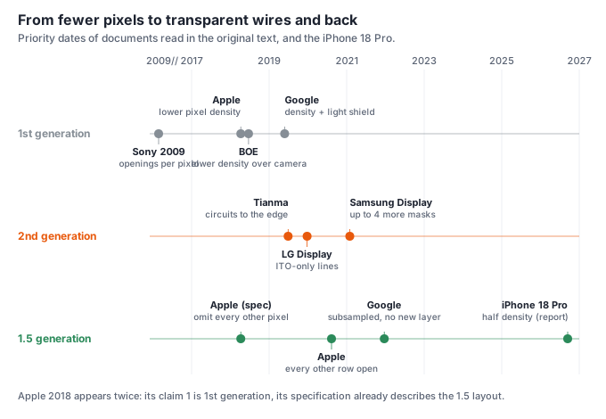
On the iPhone 18 Pro, the screen above Face ID leaves every other row of pixels empty. Under-display camera pixels went from a 1st generation that removes pixels to a 2nd generation that moves the circuits to the edge and lays transparent wiring, and the first to claim that 2nd generation was China's Tianma. But transparent wiring added masks, and Apple chose a 1.5 generation that goes back to removing pixels. Apple itself first described that arrangement in a 2018 specification and drew it in a 2020 filing.
1. Overview
1.1 Above Face ID, every other row of pixels is empty
On the iPhone 18 Pro, released in September 2026, the infrared camera for Face ID moved under the screen. It is an under-display camera (UDC). It sits at the top left of the screen, next to the clock. To the naked eye, it shows up as a barely visible, slightly darker circle.
iFixit looked at that spot under a microscope.
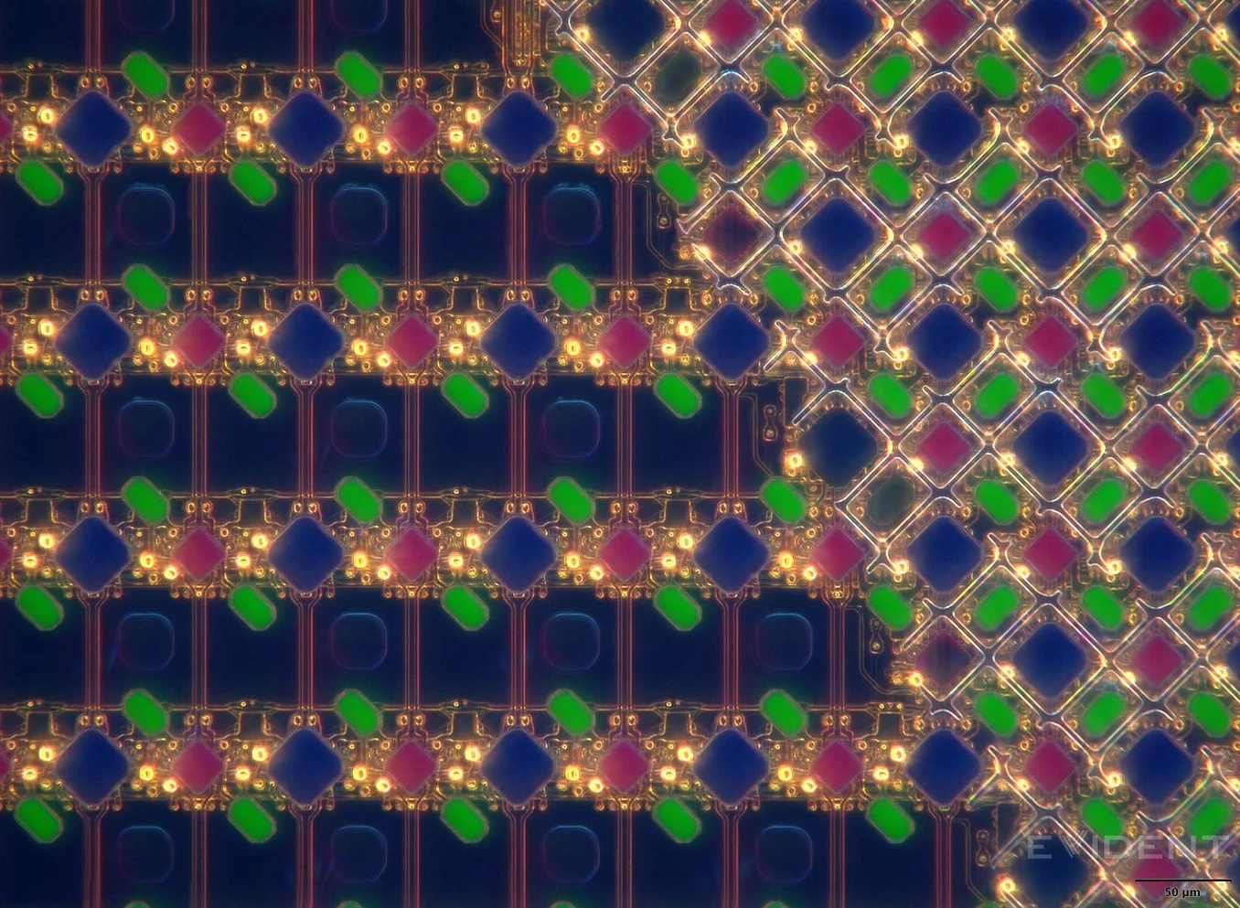
In the normal area on the right, pixels fill the space without gaps. In the area above the camera on the left, rows with pixels alternate with empty rows. iFixit wrote that “over the infrared camera, every other row of display pixels is missing,” and added that below the OLED there is a layer that appears to be “an infrared-pass filter.” 9to5Mac reported that Apple confirmed “the overall pixel density over the module is reduced by half.” To keep the area from looking dim, those pixels are driven brighter.
Remove pixels to open a light path. Simple as that answer looks, the industry went down a different road once before coming back to it. This piece traces that road back through the patent texts. The conclusion comes first.
Under-display camera pixels developed from a 1st generation that removes pixels to a 2nd generation that moves the pixel circuits out to the edge and leaves only transparent electrodes. Surprisingly, the first to claim the 2nd generation was China’s Tianma. But transparent wiring came at the price of resistance and masks, and a Samsung Display filing itself wrote that the wiring could need 4 more masks. Apple chose a 1.5 generation that goes back to removing pixels. Apple first described that arrangement in a 2018 patent specification, and in a 2020 filing drew it as a figure with every other row of pixels left empty. Google, claiming a similar arrangement for cameras in 2021, wrote in its specification a way to do it without changing the deposition mask and without adding a layer.
1.2 Scope of analysis
| Item | Value |
|---|---|
| Physical product | Microscope observations in the iFixit teardown (2026-09-20) and the 9to5Mac report (2026-09-30). These two were used only to confirm what the product looks like, not as patents |
| Patent texts | 13 documents. 7 on the 1st-generation side (Sony, Apple 2018, 2 from BOE, Google 2019, Samsung Display 2019, Tianma 2019-10), 4 on the 2nd-generation side (2 from Tianma, LG Display, Samsung Display 2021), and 2 for the 1.5 generation (Apple 2020, Google 2021). The specification of Apple’s 2018 filing was also read on the 1.5-generation side |
| How they were found | Claim conditions (camera and transmissive area + pixel circuit and transparent wiring; additional masks + transparent wiring) were entered into the Google Patents search box, and the citations and citing documents of the hits were followed |
| Deciding the 2nd-generation originator | Of the 567 documents with priority dates before the end of 2019 caught by the claim-condition search, those matching the concept of relocating the circuits were checked in the original text |
1.3 Terminology
2. The picture Apple drew in 2018
The idea of removal that the iPhone 18 Pro adopted is already in the specification of a patent Apple filed in April 2018. But it is in the specification, not the claims.
2.1 A grid with every other pixel left out
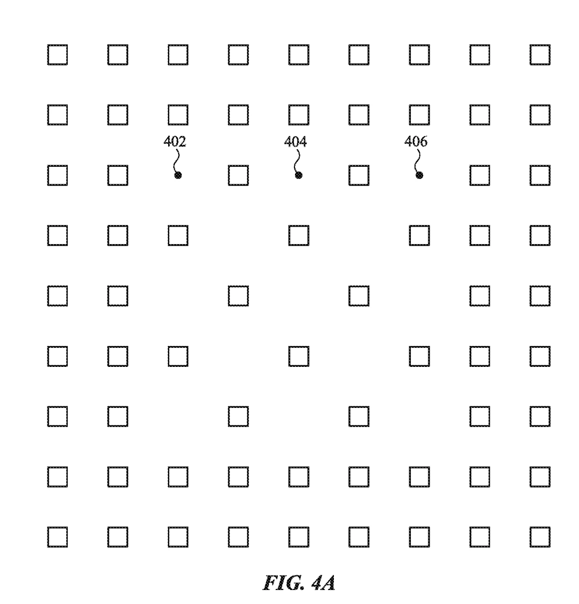
Apple’s April 10, 2018 filing (US11073712B2) covers an electronic device display for imaging through the screen. Its FIG. 4A looks like this.
The specification says this.
For example, in some embodiments, a low pixel density region can be characterized by omitting every other pixel. In another example, a low pixel density region can be characterized by omitting pixels in a geometric pattern such as, but not limited to: concentric shapes; serpentine patterns; spiral patterns; arbitrary patterns; and so on.
US11073712B2 specification (Apple, priority 2018-04-10)There is also a way to halve the density in one direction only. The specification gives as an example a region with “a pixel density of approximately 450 pixels per inch along a length of the display and of approximately 225 pixels per inch along a width of the display,” and explains that adjacent regions like this are alternated “so as to obscure the presence or appearance of lower pixel density.” Halving the density in one direction gives the same shape as leaving every other row empty. FIG. 5A of the specification also shows an arrangement that mixes in groups missing one color (red and green, green and blue) among three-color groups of red, green and blue, operating them together to produce color.
2.2 What it claimed was broader ground
Yet what Apple tied up in claim 1 is not this arrangement.
…a first pixel region having light emitting pixels with a first pixel density; and a second pixel region, offset from the first pixel region, having light emitting pixels with a second pixel density; an opaque backing below the display and defining an aperture below the second pixel region; and an optical imaging array below the aperture configured to receive light reflected from a touch input provided above the second pixel region that is transmitted through the display between two or more pixels of the second pixel region…
US11073712B2 claim 1 (Apple, priority 2018-04-10 / granted 2021-07-27)Lower the pixel density only above the camera and send light between the pixels. In this piece’s division, that is the 1st generation. The use case also centers on light reflected from a touch input, that is, under-display fingerprint imaging. In its claims, Apple’s 2018 filing stands in the 1st generation; in its specification, it had already drawn the 1.5 generation. In between, the industry made a trip down a different road called the 2nd generation.
3. The three branches at a glance
| Branch | Documents read for this piece |
|---|---|
| 1st generation | Sony 2009 · Apple 2018-04 · BOE 2018 · Google 2019 |
| 2nd generation | Tianma 2019-06 · LG Display 2019-12 · Samsung Display 2021-02 |
| 1.5 generation | Apple 2018-04 specification · Apple 2020-08 · Google 2021-12 |
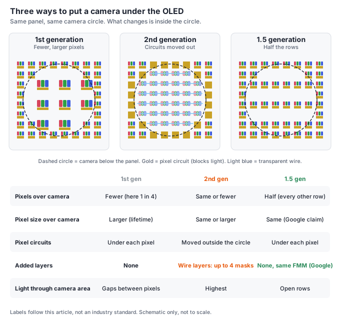
The reason for calling it the 1.5 generation is in Figure 3. On transmittance alone, the 2nd generation has the clearest advantage. Yet today’s product has come back to a point closer to the 1st generation than to the 2nd.
The model below lets you switch between the three branches.
4. 1st generation: removal
The earliest form of the idea of sending light between pixels, within the range this piece confirmed, is a 2009 Sony filing.
4.1 Sony 2009, a window at every pixel
Claim 1 of the filing Sony made with a November 2, 2009 priority date (US20110102308A1) is short.
An image display unit comprising: a display area including a plurality of pixels; an imaging unit disposed at a rear side of the image display unit behind the display area; and a plurality of light transmissive sections at locations within the display area and corresponding to the plurality of pixels, the plurality of light transmissive sections configured to separately receive light incident upon the image display unit, and pass the received light to the imaging unit.
US20110102308A1 claim 1 (Sony, priority 2009-11-02)Open a small window at each pixel position and image from behind it. Google Patents records show this one lapsed for nonpayment of maintenance fees.
4.2 Sparse only above the camera
In 2018, the idea narrowed to the area above the camera. Apple’s claim 1 (2018-04) is one such case, and BOE’s June 2018 filing family (US12266309B2) also lowered pixel density only in the area above the camera. BOE’s August 2018 filing (US11037994B2) placed transmissive parts between pixels. These two were covered in CLAIM’s BOE and Samsung Display under-panel camera patent suit analysis.
Google’s May 2019 filing (WO2020243740A1) added two things. It rearranged the circuits in the reduced-density area, and laid a light-blocking layer to prevent diffraction from the gaps between circuits. If the gaps are regular, light bends at them and produces blur and light streaks in photos. TEKER’s Why does a selfie shot through the screen come out fine? covered this problem in detail.
4.3 Enlarge pixels by as much as you remove: lifetime
Removing pixels makes the area above the camera darker. To produce the same brightness, more current has to flow through the remaining pixels, and that wears them out faster. The specification of Tianma (Wuhan)‘s October 2019 filing (CN110752242B) wrote out this chain exactly.
…to make the luminance of the second display area match the luminance of the first display area, the current of the organic light-emitting units in the second display area must be increased to compensate for luminance. This raises the current density of the organic light-emitting units in the second display area, and higher current density may shorten the lifetime of the organic light-emitting units.
CN110752242B specification, translated from the Chinese original (Tianma (Wuhan), filed 2019-10-31)So the pixels in the removal area are enlarged. A larger emitting area can produce the same brightness at a lower current density. The specification of LG Display’s 2019 filing also made the reduced-density pixels above the camera larger than those in the normal area: “a size of each of the transparent area organic light emitting diodes TOLED may be set to be greater than that of each of the opaque area organic light emitting diodes OOLED provided in the opaque area.”
This size comes up again in Section 7.
4.4 The limit of the 1st generation
Even after removal, the remaining pixels still have circuits attached. The specification of LG Display’s 2019 filing stated that limit briefly.
…four or more transistors are included in each pixel of an organic light emitting display panel which is a type of display panel. Therefore, even when a portion, corresponding to a camera, of the organic light emitting display panel is implemented as a transparent panel, a transmittance of light is reduced by transistors included in the transparent panel. Due to this, the amount of light transferred to a camera is reduced, causing the degradation in quality of an image captured by the camera.
US11751463B2 background (LG Display, priority 2019-12-24)Removing pixels alone leaves the circuits behind. Then why not take the circuits out from above the camera altogether? The 2nd generation came out of that question.
5. 2nd generation: circuits to the edge, and China came first
Place the pixel circuits outside the camera area, and leave only transparent electrodes and the emitting layer above the camera. Within the range this piece confirmed, the first to claim this concept was China’s Tianma (Wuhan), on June 28, 2019. That is half a year earlier than LG Display’s filing.
5.1 The prototype was the transparent display
The thinking behind the 2nd generation came from transparent displays. Tianma’s October 2017 filing (CN107768407B) divided the sub-pixel of a transparent display into a transmissive area, an opaque area, and an emitting area, and placed the driving circuit only in the opaque area. Gathering the circuits to one side is what makes the rest transparent. It is not for cameras, but it is the prototype of the 2nd generation.
5.2 Tianma 2019, only transparent electrodes above the camera
One year and eight months later, Tianma brought the same idea to the area above the camera. It is CN110288945B, with inventors Peng Chao (彭超) and Cui Ruili (崔锐利).
The display unit of the first display area includes a stacked first transparent electrode, light-emitting layer, and second transparent electrode. The first pixel circuit connected to the display unit of the first display area is at least partly located in the non-display area… two or more display units of the first display area are connected to one pixel circuit.
CN110288945B claim 1 summary, translated from the Chinese original (Tianma (Wuhan), filed 2019-06-28 / granted 2023-09-29)The specification also gave the reason. Placing the pixel circuit in the non-display area reduces the light-blocking area above the camera and raises transmittance. It named ITO, IZO and IGZO as transparent electrode materials. The display unit density was kept the same as in the normal area, so only the circuits were removed without sacrificing image quality. This was filed only in China.
5.3 LG Display 2019, transparent area electrode lines made of ITO alone
Half a year later, on December 24, 2019, LG Display filed in the same direction (US11751463B2, inventors JeongHyeon Choi, Sul Lee and Eunil Cho). It moves the circuits that drive the pixels in the transparent area above the camera to an outer area and connects them with transparent area electrode lines. The specification wrote that “the transparent area electrode line TEL may include only the transparent metal,” and made the cathode of transparent metal only as well. It is this transparent area electrode line that went into the representative claim.
5.4 Samsung Display was looking elsewhere at the same time
There is a Samsung Display filing from June 17, 2019 (KR102832798B1), 11 days earlier than Tianma’s. It lowered the density above the camera and placed around it a transition region where density rises gradually with distance. It is a 1st-generation refinement to keep the edge of the removal area from standing out. It has no concept of moving circuits or connecting with transparent electrodes. That is why this piece takes Tianma’s June 2019 filing as the first 2nd-generation claim.
6. The price of the 2nd generation: resistance and masks
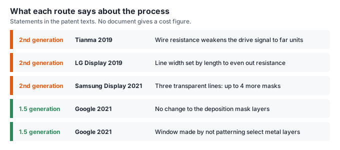
Transparent wiring saved the light, but it paid two prices: resistance higher than metal, and additional masks to pattern that wiring. Both were written into the specifications by the very companies that claimed the 2nd generation.
6.1 Resistance: the farther, the weaker the signal
Tianma had already pointed out the problem in its original filing. With the circuits at the edge, connection lines have to be run into the pixels deep inside the camera area.
A connection line is needed to connect the first display unit to its pixel circuit. Because of wiring resistance, the drive signal received by this display unit is attenuated relative to the drive signal received by the other display units.
CN110288945B specification, translated from the Chinese original (Tianma (Wuhan), filed 2019-06-28)LG Display matched that resistance with line width. The longer the electrode line, the higher the resistance, so the line width is set differently according to length to reduce differences in resistance and voltage drop between lines. Table 1 in the specification shows that when every line width is the same 5 micrometers, resistance spreads from 0 to 10 megaohms across sections depending on line length. It means each transparent line has to be designed separately for its length.
6.2 Masks: 4 more
The process-side price was counted by a Samsung Display filing. The February 1, 2021 filing (KR20220111767A, inventor Woo Min-woo et al.) is a 2nd-generation structure. It places the pixel circuits for the transparent area in an intermediate area next to the transparent area, and connects them to the anodes in the transparent area through three layers of transparent connection lines (TCL1, TCL2, TCL3) made of ITO, IZO and IGZO. It then wrote out the process for forming each connection line, one by one.
The transparent connection line TCL2 is on the same layer as the first data conductive layer but is formed with a separate mask… TCL1 is formed with a separate mask, after which an opening is made in the organic layer above it with an additional mask… TCL3 is formed with a separate mask after the spacer is formed. Forming three transparent connection lines in this way may require a total of four additional masks.
KR20220111767A specification, translated from the Korean original (Samsung Display, filed 2021-02-01)FIG. 14 of this filing lists the normal-area process with mask numbers on the left, and draws the additional transparent connection line processes separately on the right. Each extra mask adds another round of exposure, development and etching. For a camera in one corner of the screen, four rounds are added to the process for the entire panel.
7. 1.5 generation: removal again, with the same layers
While the 2nd generation kept adding transparent wiring, filings appeared on the 1st-generation side that refined the removal method. In 2020 Apple drew a figure with every other row of pixels left empty, and in 2021 Google claimed an arrangement that neither changes the deposition mask nor adds a layer. Neither moves the circuits nor lays transparent wiring.
7.1 Apple 2020, every other row left empty
Two years after the 2018 filing in Section 2, Apple filed “Displays having transparent openings” (EP4193388B1 · CN115956357B, inventor Yuchi Che et al.) with priority to a US provisional application of August 10, 2020. The drawing closest to the product in Figure 1 is in this document.
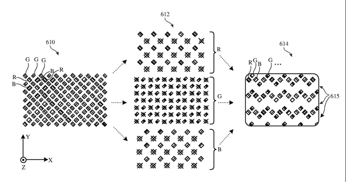
The specification describes this figure as follows: “the subpixels are removed such that there are horizontal stripes of empty pixel regions.” The remaining emissive sub-pixels “have a horizontal zig-zag arrangement following the pixel removal scheme.” It is the same shape as the “every other row of pixels missing” that iFixit saw.
There is also a figure on the circuit side.
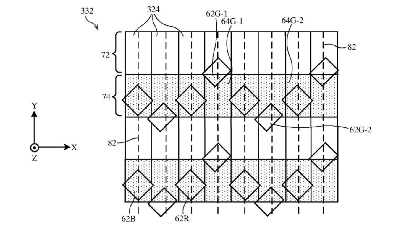
The specification explains it this way: “every other row (e.g., row 72) includes no thin-film transistor sub-pixels and every other row (e.g., row 74) includes a continuous strip of thin-film transistor sub-pixels.” The circuits are not moved outside the camera area. They are gathered into one row, and the next row is left entirely empty. Instead of laying new transparent wiring as in the 2nd generation, it removes pixels as in the 1st generation, but organizes the removal row by row.
But what this filing tied up in claim 1 is not this arrangement. Claim 1 is a device that places two sensors under transparent openings with different patterns and uses the image from one sensor to remove the diffraction artifacts in the other sensor’s image. The row-by-row arrangement is in the specification and drawings.
7.2 Google 2021, one in four with a single color
One year and four months after Apple’s 2020 filing, Google filed on December 20, 2021 (US12213364B2, inventor David Morris Hoffman et al.). It is a sub-pixel arrangement for an under-display sensor.
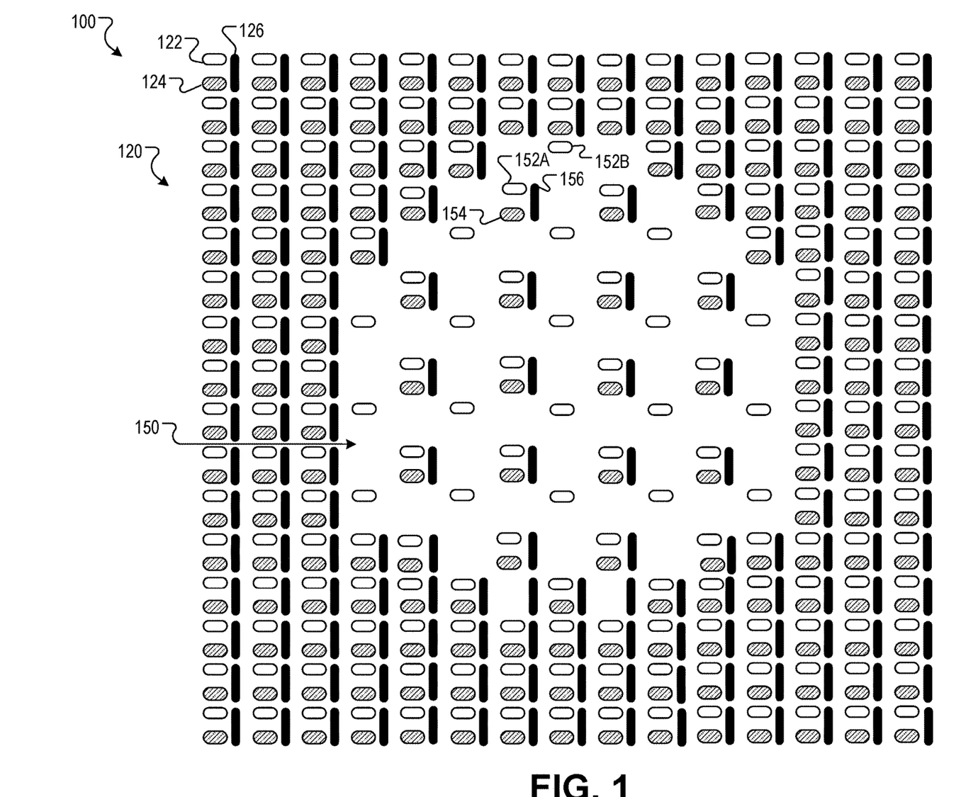
…a second area of pixel-sized regions… having a second density of LEDs that is lower than the first density of LEDs… wherein the second area of pixel-sized regions includes multiple four-pixel groupings of pixel-sized regions that are each four pixel-sized regions in size, being two pixel-sized regions high and two pixel-sized regions wide, each four-pixel grouping of pixel-sized regions including: a pixel of the first type of pixel that has… (i) a first sub-pixel comprising an LED of the first color, (ii) a second sub-pixel comprising an LED of the second color, and (iii) a third sub-pixel comprising an LED of the third color… and a pixel of a second type of pixel that has… (i) a sub-pixel comprising an LED of the third color, (ii) without any LED of the first color, and (iii) without any LED of the second color.
US12213364B2 claim 1, excerpt (Google, priority 2021-12-20)Two pixels in four cells. The density is halved. The specification adds three things.
First, the wiring is reduced to match where pixels were removed. “Data lines and rows that drive the sub-pixels of the third color may be reduced by 50% using staggered connections to emissive pixels.”
Second, the metal data lines crossing the empty positions are not kept straight. The specification wrote that the data lines bending between pixels “follow a non-linear path that reduces flare” (patent FIG. 5). Straight lines in a regular row bend light like a diffraction grating. Bending the lines breaks up that regularity. It solves the diffraction problem from Section 4 with the shape of the wiring rather than a light-blocking layer.
The third is where it parts ways with the 2nd generation.
The display panels described above may transition from an RGB triplet arrangement to a subsampled pixel arrangement without a change to the deposition mask layers… In an under-display sensor region of the display, some of the sub-pixels may be omitted by not patterning select metal layers to create a transparent window in a region.
US12213364B2 specification (Google, priority 2021-12-20)The 2nd generation opened the window by patterning additional transparent wiring layers. The 1.5 generation opens the window by not patterning part of the metal layers that were already there. The masks the two documents talk about are of different kinds. What Samsung Display counted as “four additional” are photomasks for patterning wiring layers, and what Google says is unchanged is the deposition mask for the emitting layer. But the direction clearly splits. One side adds layers, and the other does not.
Pixel size splits too. As seen in Section 4.3, the removal area had the option of enlarging pixels to protect lifetime. Google instead tied size down in claim 1: the three-color pixels above the camera occupy “a same amount of space within the grid of pixel-sized regions” as the three-color pixels in the normal area. According to the 9to5Mac report, the iPhone 18 Pro took the route where “Apple increases the brightness of these pixels to compensate” rather than enlarging them. How lifetime was handled at that price could not be found in public documents.
7.3 The documents Google stands on
The Google patent cites 9 documents. Those the applicant cited directly include Apple’s 2018 publication (US20190310724A1, that is, US11073712B2 from Section 2) and Google’s own 2019 filing, listed together with BOE’s 2018 filing and 4 Samsung Display documents (3 of them cited by the examiner). Google, in effect, claimed for cameras as a 2×2 arrangement, three and a half years later, the “omitting every other pixel” and the “incomplete subpixel groups” missing one color from the Apple specification seen in Section 2.
Tianma’s 2019 original 2nd-generation filing is not among these 9.
7.4 Apple’s choice
Back to Figure 1. The screen above the camera on the iPhone 18 Pro halved its pixel density, and the remaining rows of pixels still carry all three colors and their circuits. It is not the 2nd generation with circuits moved to the edge, but the 1.5 generation that goes back to removal.
The 2nd generation has the best transmittance. But transparent wiring brings resistance and, as the Samsung Display filing itself wrote, raises the mask count by up to four. Amid that burden, Apple chose the 1.5 generation. And that arrangement points in the same direction as what Apple first described in its 2018 specification and drew as a row-by-row figure in its 2020 filing.
8. Counterevidence and limitations
This piece did not determine which patent the iPhone 18 Pro practices. Whether it is Apple’s own patent, whether it has any relationship to the Google patent, and who made the panel could not be found in public documents. What this piece says goes only as far as this: the product uses a 1.5-generation-type arrangement, and that arrangement was first written down in Apple’s specifications (2018 and 2020) and Google’s claims (2021).
No document proves that “they moved to the 1.5 generation because of masks.” The resistance and mask burden of the 2nd generation, and the statements that the 1.5 generation adds no layer and keeps the deposition mask unchanged, are all in the patent texts. But no company wrote “so we abandoned the 2nd generation.” “Apple chose the 1.5 generation” in Section 7.4 is this piece’s reading, placing those facts side by side.
This piece does not attribute intent to design around. It is a fact that Tianma’s original filing is not among the documents cited by the Google patent. But whether that was because Google did not know of it, avoided it, or was solving a different problem in the first place cannot be told from the documents.
The finding on the 2nd-generation originator holds within the range checked. A Chinese-language filing that does not show up in English searches could be earlier.
The 1st, 2nd and 1.5 generations are this piece’s division. They are not names the patent texts use for themselves, nor an official industry classification.
The drawings that most resemble the product are FIGS. 6 and 9 of Apple’s 2020 filing (Figures 5 and 6 in this piece). The Google claim places, within each group of four cells, a pixel that keeps only one color, so its arrangement differs from the product. Apple’s 2020 filing also wrote that arrangement in the specification, not the claims. This piece does not say the product was made according to these drawings. There is no material to compare it sub-pixel by sub-pixel.
9. Conclusion and implications
The history of under-display camera pixels is not a road that only went forward.
The 1st generation removed pixels. The 2nd generation moved the circuits to the edge and laid transparent wiring to push transmittance as far as it would go, and its first claim was China’s Tianma in June 2019. But transparent wiring came at the price of resistance and masks, and a Samsung Display filing put that price as “four additional masks.” The answer Apple put out in 2026 was to go back to removal. The first picture of that answer was in Apple’s own 2018 specification, and Apple’s 2020 filing went as far as drawing a figure with every other row of pixels left empty. In 2021 Google claimed an arrangement for cameras that adds no layer.
The structure with the best transmittance does not necessarily become the mass-production structure. In the texts read for this piece, what separates the 2nd generation from the 1.5 generation was not the pixel arrangement drawing but the process table.
Two things are worth watching. One is how claims among Apple, Google and the panel makers overlap around the 1.5-generation arrangement. Filings that vary slightly where pixels are removed and how the wiring is shaped keep piling up, and there is also a 2023 Samsung Display filing (US20240407209A1) in which the examiner cited the Google patent. The other is whether the 2nd generation will disappear. If a process comes along that lightens the mask burden, the 2nd generation, ahead on transmittance, could return. When that happens, the side holding the original claim is China.