Inducing nanocracks to secure both efficiency and stretch in an OLED
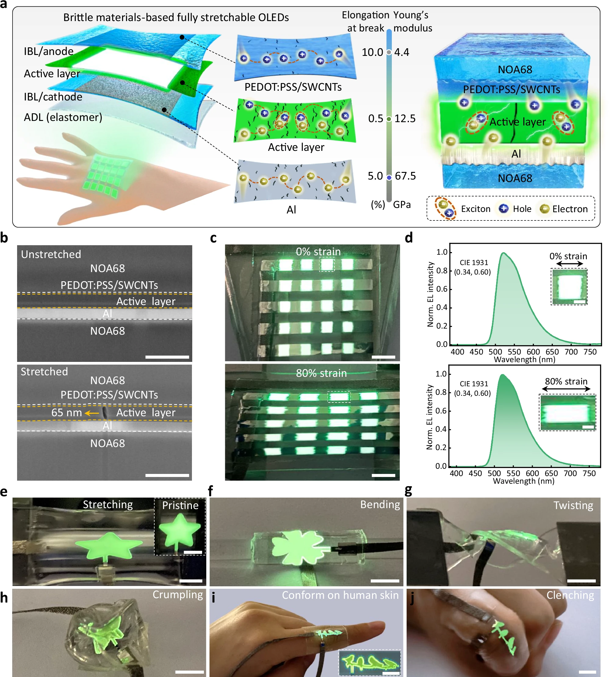
Stretchable OLED research has so far been entirely about stopping cracks from forming. A Northeast Normal University group went the other way. They designed where and in which direction the cracks would run, standing 65-nanometre-wide cracks vertically and only inside the emissive layer. At 1/10 of a visible wavelength they are invisible, and the vertical current path is not broken. An external quantum efficiency of 24.7% passes the previous record for a stretchable device.
DOI 10.1038/s41467-026-76917-2The most troublesome component in making a screen that stretches is the emissive layer. The emissive layer of an OLED on sale today is small-molecule organic material laid down by vacuum deposition, and this material breaks before it stretches even 1%. The elongation at break of the active layer measured in this paper is about 0.5%. To talk about a screen that wraps around a wrist while the layer that actually emits light shatters at 0.5% is to have no discussion at all.
So this field has long asked “how do we keep cracks from forming?” The Northeast Normal University group inverted the question. Cracks will form anyway. In that case, let us design where, how narrowly and in which direction they form.
To give the result first, the device delivered a current efficiency of 85.7 cd/A and an external quantum efficiency of 24.7%. The previous best for a stretchable small-molecule OLED was 47.9 cd/A and 17.0%, so efficiency was not sold to buy stretchability. Both were raised together.
1. Why insist on a material that breaks at 0.5%
First, why this awkward material is insisted upon has to be set out.
Small-molecule organic semiconductors have high colour purity and good film uniformity. Above all, several layers can be stacked precisely by vacuum deposition. That is what lets today’s commercial OLEDs pile hole injection, hole transport, electron blocking, emissive and electron transport layers on top of each other at the nanometre scale. Devices made from polymer semiconductors are generally an order of magnitude lower in emission efficiency.
So a stretchable display cannot discard this material if it is to become a real product. The moment it is discarded, efficiency goes with it.
2. The two routes so far, and what they cost
Existing approaches fell broadly into two.
Geometric stretching (gs-OLED) leaves the device itself rigid and solves it through shape. A flexible device is attached to a pre-stretched substrate and released to form wrinkles, or rigid islands are joined by stretchable interconnects. The advantage is that the materials can be used as they are, but the surface ripples or the emission is broken up island by island, so the screen does not look uniform.
Intrinsic stretching (is-OLED) blends the small molecules with an elastomer or polymer to make the emissive layer itself stretch. The screen is uniform, but the cost is plain. What makes small molecules efficient is the dense π–π stacking of the molecules, and the moment an elastomer is blended in, that stacking is disturbed. Efficiency and stretchability eat into each other.
In numbers, the best record for this route was a current efficiency of 47.9 cd/A, an external quantum efficiency of 17.0%, maximum elongation of 60%, and 100 cycles at 20% strain.
3. Not blocking them, making them
The route the group took is a third one. The paper calls it active crack engineering.
The idea is simple. Rather than stretching the device whole, the emissive layer is split into a great many microdevices at very narrow spacing. The gaps between the split pieces absorb the stretch while the pieces themselves stay as they were and emit light. Those gaps are the induced nanocracks.
For this strategy to hold, two things have to be true at once.
First, the gaps must not be visible. The measured crack width is about 65 nanometres. Visible wavelengths are 400 to 700 nanometres, so the crack is around 1/10 of a wavelength, and no dark diffraction fringes arise. It is not a visible fissure but something closer to optically non-existent.
Second, the current path must not be broken. Charge in an OLED flows up and down. If cracks run only vertically, they divide the emissive layer sideways while leaving the vertical path intact. Conversely, the moment a crack lies down horizontally, electrode and emissive layer part and the device dies. So the real task of this work is not “making cracks” but “standing the cracks vertically.”
4. Covering with a buffer layer above and below
The layer structure reveals the design intent.
At the very bottom is the strain adaptation layer (ADL), a 3M VHB 4918 elastomer with an elongation at break of 860%. It is the layer that actually takes the stretch. The trouble is that this layer has a modulus of 15.6 kPa while the whole functional stack going on top of it has a modulus of 33.6 GPa. Butt two layers 2 million times apart and stress piles up at the boundary.
So an interfacial buffer layer (IBL) goes between them. It is NOA68, a UV-curing thiol-ester adhesive, sitting between the two at a modulus of 127.4 MPa. It forms Al–S bonds with the aluminium cathode and C=S bonds with the anode, so the interfaces interlock physically.
The key is that this buffer layer was laid on above the functional stack as well as below it. The comparison of three structures is the clearest passage in this paper.
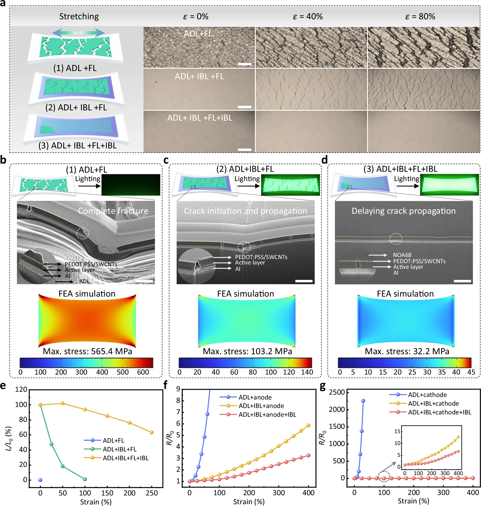
The maximum stress at the centre of the device, computed by finite element analysis, comes down like this.
| Structure | Max stress (80% strain) | Result |
|---|---|---|
| adaptation + functional | 565.4 MPa | cracks tens of micrometres wide at 40% strain, 46.4% of the area |
| adaptation + buffer (below) + functional | 103.2 MPa | crack width reduced, but the upper layer left unguarded |
| adaptation + buffer + functional + buffer | 32.2 MPa | no surface cracking at 80% strain, only 65 nm cracks inside the emissive layer |
Stress fell by a factor of 17.6. And one value in the luminance curve catches the eye. The structure covered above and below is at 102% of its initial luminance when stretched 50%. It got brighter on being stretched, which reads as the result of the layer spacing changing minutely in a top-emitting structure and altering the optical cavity condition.
The electrode resistance is worth noting too. At 400% strain the anode resistance is 3.3 times its initial value and the cathode 6.8 times. That means charge injection is maintained, and it is the physical basis for the device staying lit up to 250%.
5. Electrode asymmetry sets the crack direction
What stands the cracks vertically is not the buffer layer but the difference in properties between the upper and lower electrodes. The group showed this by making three combinations.
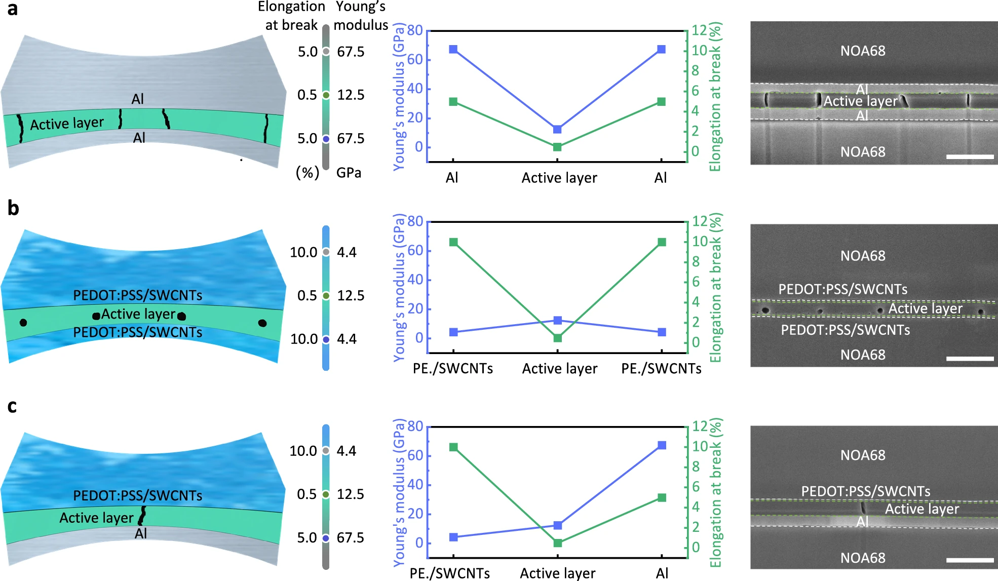
Aluminium on both sides (both stiff). Aluminium, at 67.5 GPa modulus and 5% elongation at break, presses the emissive layer, at 12.5 GPa and 0.5%, from above and below. A great many vertical through-cracks form. The crack direction is right but the density is excessive.
PEDOT:PSS/carbon nanotube on both sides (both soft). At a modulus of 4.4 GPa it is close to the emissive layer, with 10% elongation at break. There are no interfacial cracks, but instead directionless round cracks scatter inside the emissive layer. Where the current path will be cut cannot be predicted.
Soft below, stiff above (asymmetric). Anode 4.4 GPa and 10%, cathode 67.5 GPa and 5%. That gradient gives the stress a direction, and the cracks grow vertically only, with no lateral offset. This combination was adopted.
In short, the buffer layer reduces the magnitude of the stress, and electrode asymmetry sets the direction of the cracks. Each does a different job.
6. A window of 140 seconds of ultraviolet
The buffer layer is a UV-curing material, so exposure time is itself a process variable. This is the passage that lands most concretely on the industry side.
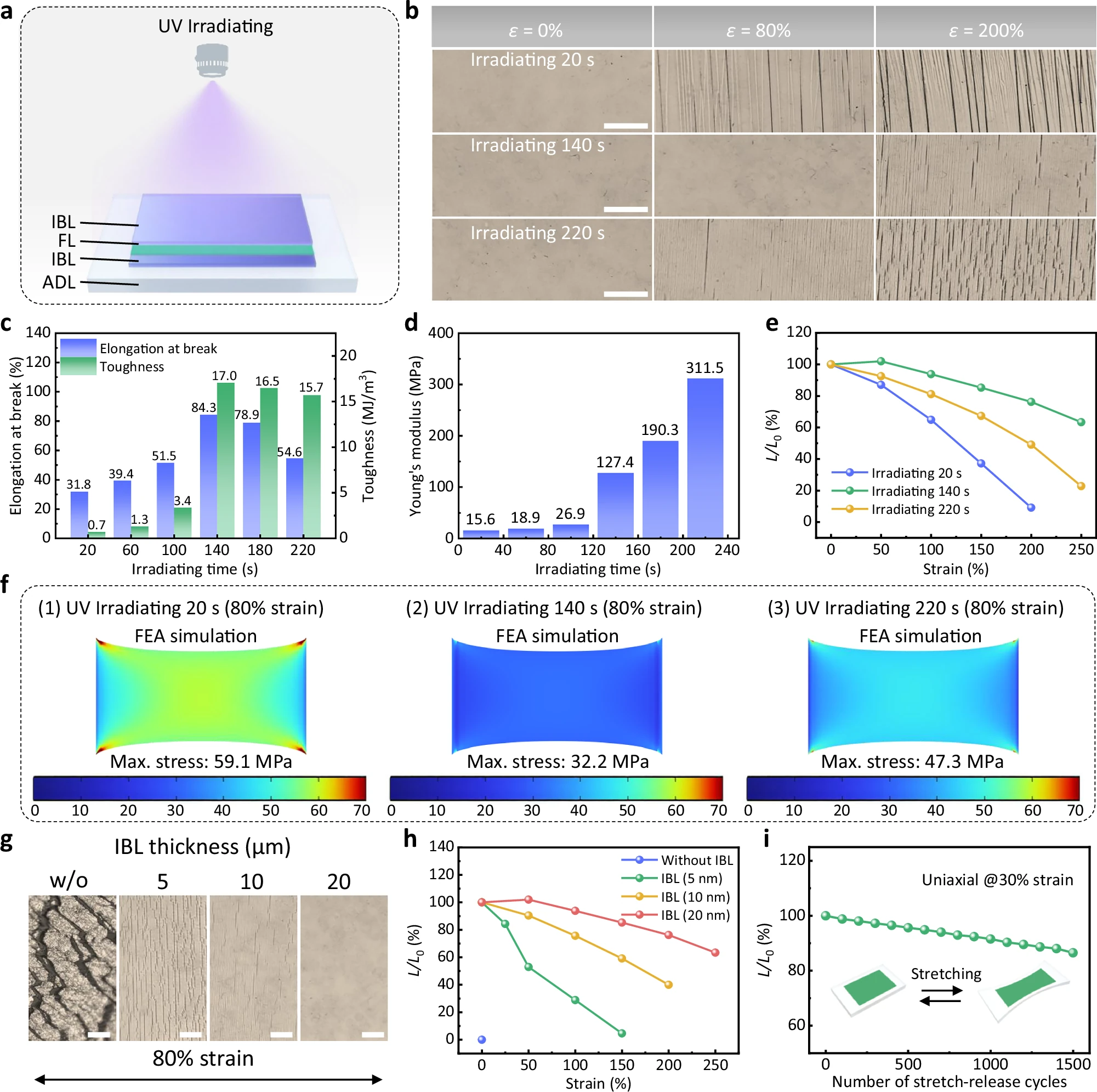
Expose for only 20 seconds and crosslinking is insufficient, giving an elongation at break of 31.8% and toughness of 0.72 MJ/m³. Stretch it only 80% and cracks spread across the whole device surface.
At 140 seconds it peaks, at 84.3% elongation and 17.0 MJ/m³ toughness. The polymer chains are entangled just enough to slide past each other and let stress flow away. Here the device shows only a few fine lines on the surface even at 200% strain.
Push to 220 seconds and over-crosslinking sets in. The chains are tied so they cannot move, elongation at break falls to 54.6%, and the modulus alone shoots up to 311.5 MPa. Stress concentrates at the crosslinks, creating the very place where fracture starts.
Look at modulus alone and it seems to keep improving, while the device gets worse. It is the kind of problem missed when a process is optimized around a single material property.
Buffer layer thickness has to be set alongside. As it goes from 0 to 20 micrometres the microcrack area falls, and at 20 micrometres it holds 76.2% luminance at 200% strain.
7. Four colours, and repetition
If the strategy worked only for one particular emitter, it would end with a single paper. The group changed the emitter and rebuilt the same structure.
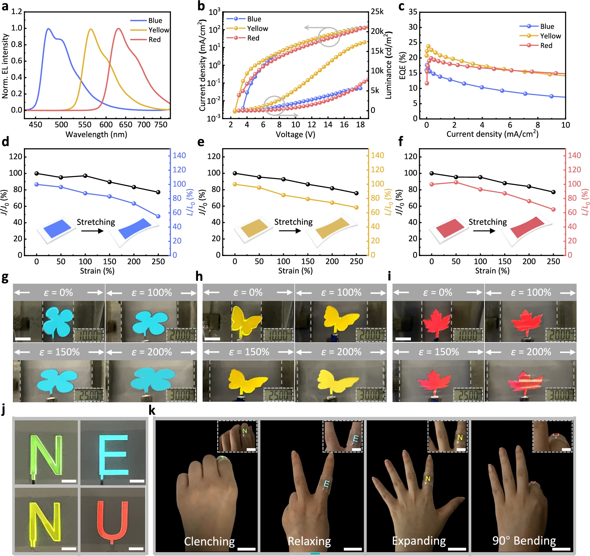
| Colour | Emitter | Peak wavelength | Turn-on voltage | Max luminance | Max EQE |
|---|---|---|---|---|---|
| green | Ir(ppy)3 | 520 nm | 2.5 V | 16,050 cd/m² | 24.7% |
| blue | Firpic | 472 nm | 3.5 V | 5,660 cd/m² | 17.7% |
| yellow | PO-01 | 560 nm | 2.5 V | 17,320 cd/m² | 23.9% |
| red | Ir(piq)3 | 628 nm | 3.0 V | 7,940 cd/m² | 19.9% |
All three colours kept over 90% of their current density and over 80% of their luminance after 100% strain, and the patterned device held even emission at 200% strain.
Cyclic durability is as follows.
- 86.5% luminance retained after 1,500 cycles of 30% uniaxial tension
- 81.2% after 1,500 cycles of 20% biaxial tension
- 90.4% at a bending radius of 1 mm
- 80.4% after 10,000 cycles of bending at a 5 mm radius
8. Reading the number 250% precisely
The most striking figure in this paper is 250%, and it deserves to be read precisely.
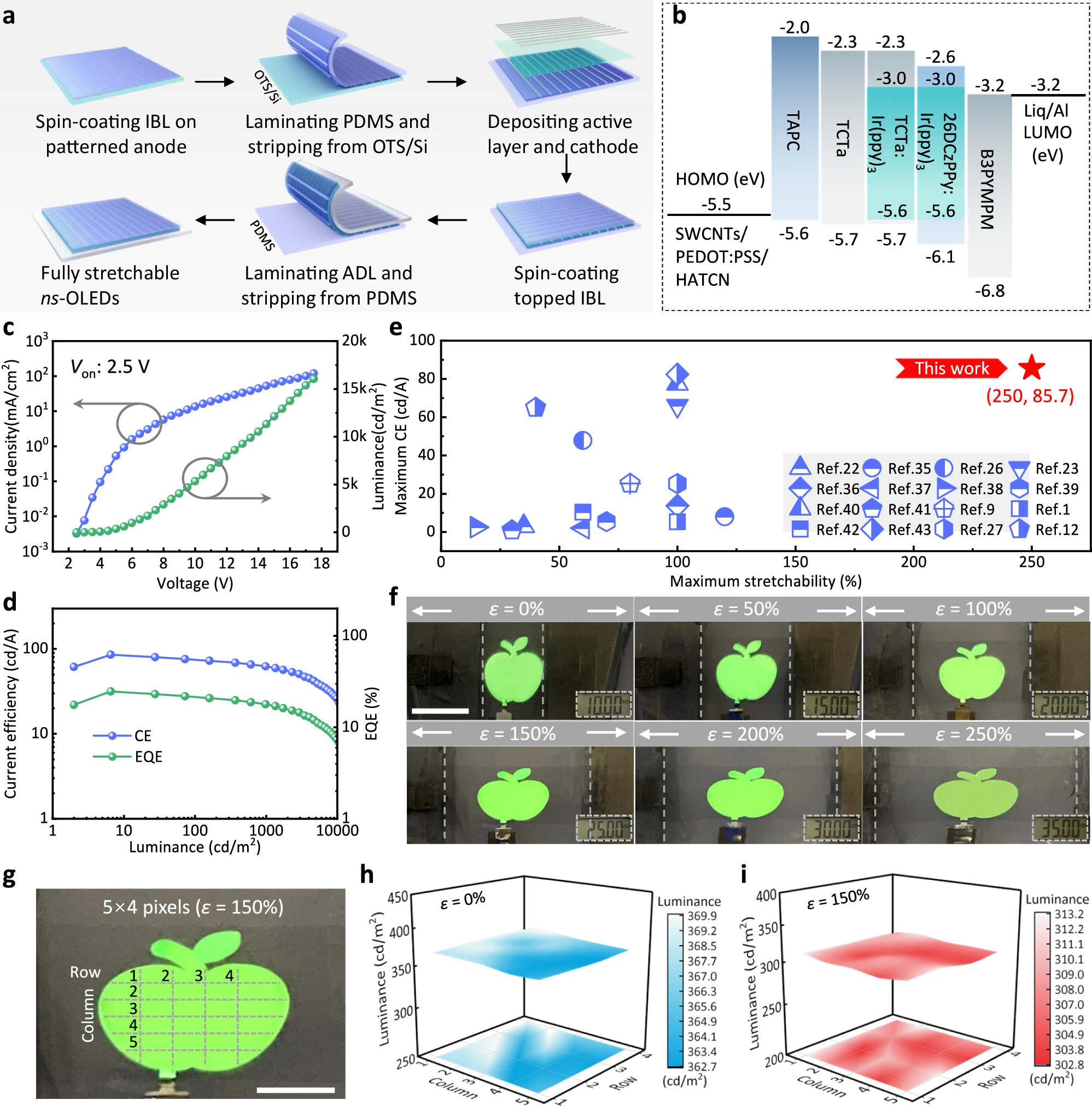
The paper states this value as “a state in which the whole electrode area is expanded 250%, at which point the elongation of the emitting region itself is about 50%.” That is, when the whole device is stretched two and a half times, the strain the light-emitting part actually experiences is a fraction of it. The elastomer and interconnects outside the emitting region take up the stretch first.
That does not make 250% an inflated figure. What a device attached to a wrist or a finger joint actually experiences is the deformation of the whole module, and whether the screen stays lit under that condition is what matters. But reading it as “the emissive layer stretched 250%” is wrong. Had the emissive layer stretched 250%, it would contradict the paper’s own premise of 0.5% elongation at break.
For the same reason 83.2% and 63.4% have to be kept apart. What is retained at 250% strain is 83.2% on a current efficiency (cd/A) basis, and 63.4% on a luminance basis. It is not that more current was pushed through to preserve brightness; it is that this much efficiency per unit current remains.
One more thing. This paper is an Article in Press. The accepted manuscript has been released ahead of the formal version, so there is room for figures to be adjusted in the final edited version.
9. Where it touches the industry
The most industrial sentence in this work is neither the efficiency nor the elongation; it is in the materials list.
The device’s organic layers are HATCN · TAPC · TCTa · 26DCzPPy · B3PYMPM · Ir(ppy)3. All commercial materials. The buffer layer NOA68 and the adaptation layer 3M VHB 4918 are catalogue items too, and the deposition is conventional high-vacuum thermal evaporation as it stands.
This contrasts with a good many stretchable device papers that presuppose custom-synthesized materials. If the performance came not from developing a new material but from changing how already-used materials are stacked, then no new procurement burden falls on either the materials maker or the panel maker.
There is of course more to get past. How to put encapsulation onto a top-emitting structure, and whether pixels can be driven by thin film transistors in a stretched state, are outside this paper’s scope. The 4×5 pixel array is not actively driven.
Even so, moving the question from “keep cracks from forming” to “decide where the cracks will run” is this paper’s contribution. If a material with 0.5% elongation at break can be used in a device that stretches 250%, there are plenty of brittle materials besides emissive layers to which the same logic would apply.
- elongation at break
- How far a material stretches just before it snaps. The small-molecule organic emissive layer is 0.5%, the elastomer adaptation layer of this device 860%.
- active crack engineering
- An approach that, rather than blocking cracks, induces them by designing their position, width and direction. The core concept of this paper.
- interfacial buffer layer (IBL)
- A layer of intermediate properties placed between two layers of greatly differing modulus to distribute stress. Here it is the UV-curing adhesive NOA68.
- finite element analysis (FEA)
- Numerical analysis that divides a structure finely to compute the stress distribution. Used here to compare the maximum stress at the centre of the three structures.