Optical Communication and ToF Ranging with a Micro-LED Display
Micro-LEDs can be switched on and off on a nanosecond scale, so a screen is thought able to double as a communication link and range sensor. Researchers at the University of Strathclyde and the University of Edinburgh tried it with a 128×128 display. With the same pixel light they sent 0.68 Gbps while measuring distance to an object 80 cm away with a 4 cm error, and the two functions barely eroded each other. What set the ceiling was not optics but driver chip wiring.
DOI 10.1364/oe.606550The front of a phone holds three parts. There is the screen, there is a range sensor that measures the contours of a face, and there is a module that sends and receives data wirelessly. The three run separately, at different wavelengths, on different chips. The range sensor usually fires a laser, and communication uses radio.
With the arrival of Micro-LED came the idea that these three could be merged into one. Micro-LEDs made from inorganic gallium nitride (GaN) can switch on and off on a nanosecond scale. The human eye cannot see that flicker at all, but a detector can. In that case the light of the screen’s pixels could itself become a communication signal, and become the illumination that measures distance.
A joint study by the University of Strathclyde and the University of Edinburgh, published in Optics Express this week, tried doing both at once on a single display. A 128×128 Micro-LED display sent data at 0.68 Gbps while, at the same moment and with the same pixel light, measuring distance to an object 80 cm away with a 4 cm error.
And what deserves more attention in this article is what comes next. The two functions shared the same light, yet barely eroded each other. What held the speed back was not the optics but the wiring of the display driver chip.
1. Why a screen wants to double as a sensor
In today’s phones, face recognition is done with an infrared laser and separate optical parts. The laser light is shaped by a part such as a digital micromirror, fired out, and the light coming back is received. Wireless communication runs in an entirely different radio band.
Having separate parts means each takes up its own space. That is why an industry trying to stretch the screen to the very edge of the front has worked so hard to push cameras and sensors under the screen.
If the display doubles as illuminator and transmitter, the story changes. The paper’s introduction sums up this direction as follows. As Micro-LED displays have become able to operate at high speed, the possibility has opened that the display itself takes on the roles of several subsystems and reduces the need for separate parts. It draws a line, though: Micro-LED displays are only now entering commercialisation, and using them for communication and ranging is still a research topic.
2. What a nanosecond pixel does
The condition that a screen has to be fast was in fact met long ago. The human eye follows only tens of changes per second, so a screen only needs to be a little faster than that. Micro-LEDs are thousands of times faster than that.
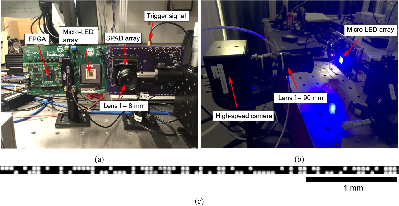
The display used in this experiment is the CMOS-driven 128×128 Micro-LED array the same group reported earlier. It can change patterns at up to 500,000 frames per second and can emit optical pulses 4 nanoseconds wide. The chip is controlled by an FPGA.
This speed creates two uses.
- Optical wireless communication (OWC): switching a pixel on and off is itself used as 1 and 0. Point-to-point optical communication with Micro-LEDs has already been reported at around 10 Gbps
- Time-of-Flight (ToF) ranging: fire a short pulse of light and measure the time it takes to hit an object and come back, and you get the distance. Face recognition, lidar and games console motion recognition work this way
Many studies have done the two separately. This is the first time both have been done at once on a single display, the paper writes.
3. Two signals overlaid within one frame
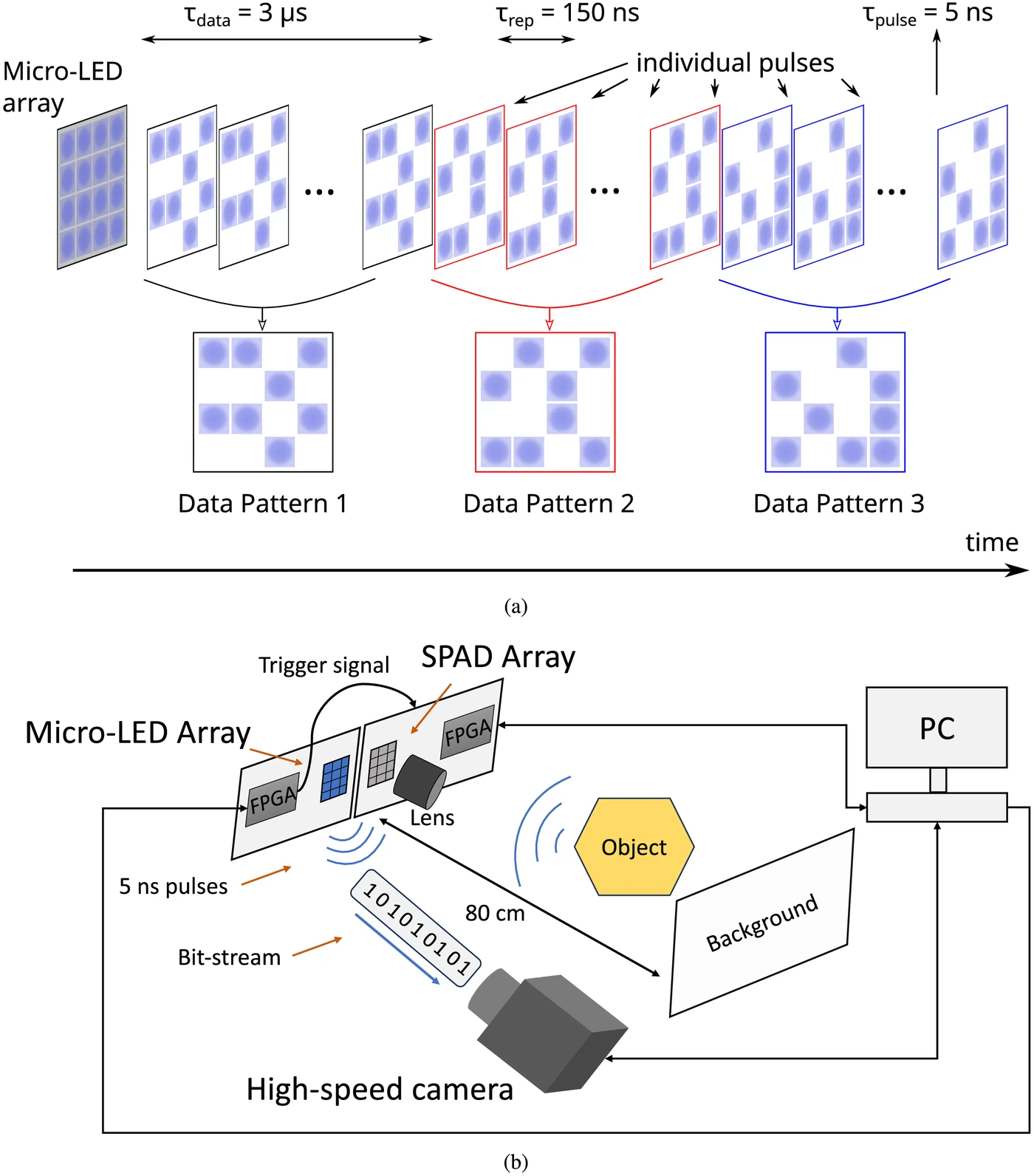
The key was the firmware. The team modified the FPGA firmware to display binary patterns at 333,000 frames per second while overlaying short pulses in which every pixel lights at the same instant.
Unpacked, the structure is this. A single data pattern stays up for 3 microseconds. Within those 3 microseconds the pixels flash as a pulse once every 150 nanoseconds. The pattern is used for communication, and the pulses are used for ranging. Pixels that are on glow in pulses and pixels that are off stay dark, so the pattern information rides on the pulses intact.
The pulse width differed between experiments. In a preliminary experiment with a single SPAD it was 5 nanoseconds, and in the SPAD camera experiment this article covers it is 40 nanoseconds, because the camera required a sync pulse of at least 20 nanoseconds. Even so, the paper writes, the ranging accuracy came out similar to the preliminary experiment.
There are also two receivers. The communication data is received by a high-speed camera running at 800,000 frames per second, and the distance information by a SPAD (single-photon avalanche diode) camera. A SPAD is a detector that responds even when a single photon arrives, so it can measure the arrival time of weak returning pulses with 32-picosecond resolution.
4. Communication at 0.68 Gbps, with the eye wide open
Take the communication results first.
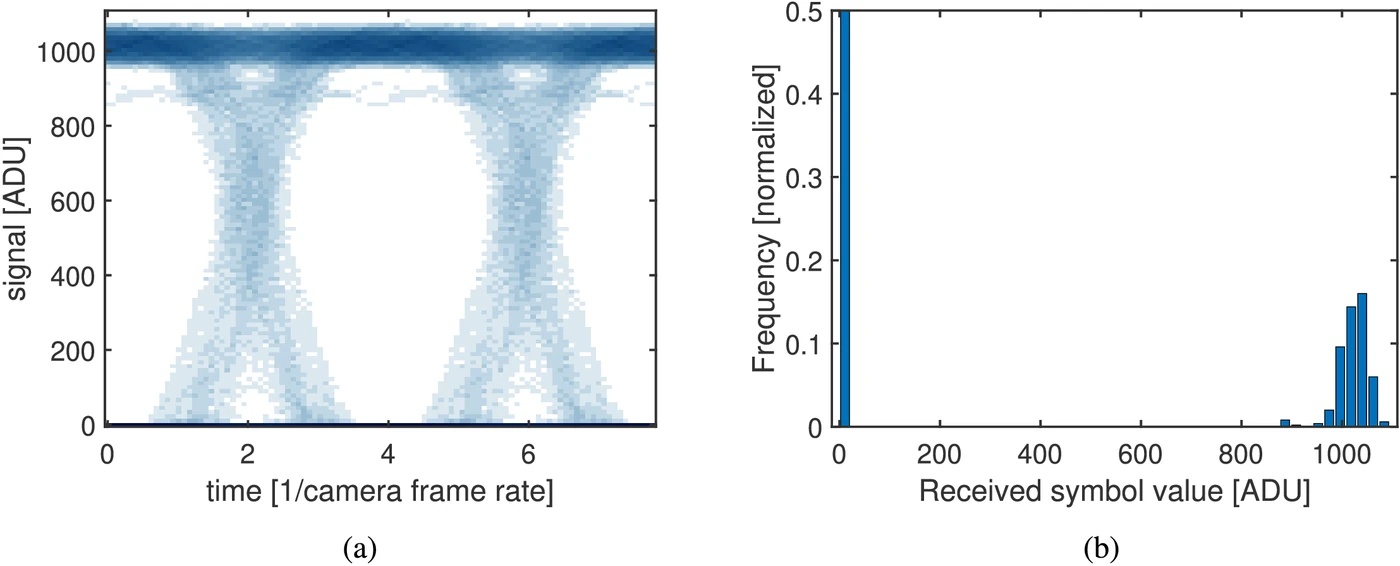
Of the 128×128 array, a 16×128 region was used. Each pixel carried a pseudo-random bit sequence (PRBS) by on-off keying (OOK), running 500 frames. A high-speed camera captured 10,000 frames, from which the brightness changes of each individual pixel were extracted and turned back into bits.
The bit error rate of every active pixel was below the standard forward error correction threshold. The combined data rate across the whole 16×128 region is 0.68 Gbps, which converted to screen area is 13.3 Gbps per square centimetre. This figure is the sum of 2,048 pixels each sending 333,000 bits per second.
The eye diagram shows the result. It is a picture that captures the quality of a communication signal in a single image, and the wider the “eye” between 0 and 1 is open, the less the two are confused. The eye is clearly open, and the distribution of received signals also split cleanly into a 0 side and a 1 side.
5. Distance to within 4 cm at 80 cm
The distance side was measured like this.
The Micro-LED array fires pulses like a flood light illuminating the whole scene. When photons that have hit an object and come back enter a SPAD pixel, an on-chip time-to-digital converter records the arrival time. Accumulating 10,000 frames of this builds a distribution of photon arrival times for each pixel.
With a pulse width of 40 nanoseconds, light travels 12 metres in that time. There is a reason centimetre-level results still come out. The team took a sheet of white paper at 30 cm as a reference and measured how far the peak had shifted by cross-correlating the reference distribution with the actual scene distribution. Fitting the peak position with a Gaussian function catches shifts far smaller than the width of the distribution.
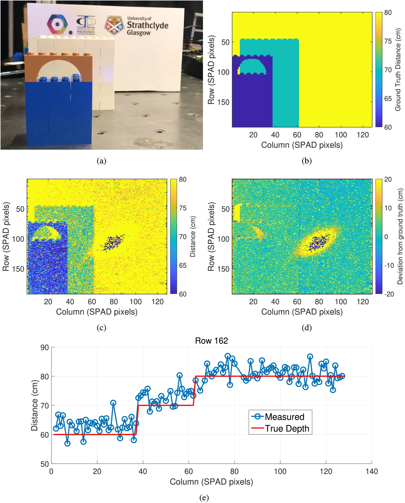
There were two test scenes. A honeycomb structure was placed at 60 cm and an arch built from LEGO bricks at 60 and 70 cm, with a white background standing behind at 80 cm.
| Scene | Pixels excluded | Root mean square error | Standard deviation |
|---|---|---|---|
| Arch, single cross-section row | Chosen to avoid defect areas | 3.6cm | 2.9cm |
| Arch, whole | 16.7% | 4.0cm | 3.6cm |
| Honeycomb, whole | 16.1% | 4.4cm | 4.3cm |
6. The two did not erode each other
This is where the point of the study lies.
The communication signal and the ranging pulses are the same light from the same pixels. Ordinarily one would expect one side to become noise for the other. The result was otherwise.
On the communication side, overlaying the pulses did not worsen the bit error rate. The team confirmed this by comparing with earlier results from the same display used for communication alone, without pulses. Judging from the eye diagram and the histogram, what limited the data rate was not the signal-to-noise ratio.
Then what did limit it? The paper names three limits.
- Delay in the wiring that the digital control signals pass through on the FPGA
- The frame rate of the receiving high-speed camera
- Parasitic capacitance in the driver chip. In pulse mode, AC current charging the parasitic capacitance restricted the number of pixels that could be switched on at once
The third left its mark on the experimental design too. Only a 16×128 region, not the whole 128×128 array, was used for communication, because the optical output in pulse mode peaked at around 1,000 active pixels. The 2,048 pixels of the 16×128 region are each on half the time, so about 1,000 pixels are lit at any instant. Light more than that, and output drops as the driver chip charges the parasitic capacitance.
The limit on ranging was not optical either. What held accuracy back was shot noise arising from too few photons, not the pulse width or the time resolution. The paper writes that this improves by pulsing more LED pixels. Yet what prevents lighting more is precisely the parasitic capacitance above.
The limits of the two functions converge on the same place. It is neither the optics nor the detector but the electronic design of the display backplane and driver chip. That is why the team wrote in its conclusion that “The performance limits for both ranging and data display are dominated by device engineering challenges such as signal routing or parasitic capacitances on the power distribution network.”
The team also set out the condition under which the two functions are fully separated. Carrying the communication signal in Manchester coding gives complete orthogonality but halves the data rate. Without it, interference can arise when the data contains long runs of 0s, which the paper writes can be solved with low-overhead coding.
7. Neither is a record
There is something to point out here. Looking at the comparison table of prior work the paper itself compiles, this result is not the record for either function.
| Study | Light source | Display | Data rate | Ranging accuracy | Distance | Acquisition time |
|---|---|---|---|---|---|---|
| Same group, earlier work | Micro-LED | ✓ | 5Gb/s | No ranging | ||
| Laser optical communication | Laser diode | 35.6Gb/s | No ranging | |||
| LED communication + 3D (2022) | Conventional LED | 400kb/s | 2cm | 0.25m | 0.2 s | |
| Same group, preliminary result | Micro-LED | ✓ | 80Mb/s | Under 1cm | 0.15m | |
| This study | Micro-LED | ✓ | 0.68Gb/s | 4.4cm | 0.8m | 300 s |
The data rate is lower than when the same display did communication alone, the ranging accuracy is worse than the preliminary result, and the acquisition time is the longest in the table. The paper does not hide this either. Instead it says the report covers “an operational regime that has not been explored before”, meaning that doing gigabit-class communication and 3D ranging at once on a single Micro-LED display is a first.
8. Between the abstract and the body
When reading this paper from the industry side, five things must be distinguished. They are what you miss if you read only the abstract.
First, no video was shown. The abstract presents a display that “can act as a normal video display while also sensing objects in its environment”. Yet what was put on screen in the experiment was binary data patterns for communication. In the conclusion the team calculates that using the binary pattern updates at 333,000 frames per second as pulse-width modulation could display video at 100 frames per second with 11-bit greyscale, and leaves that to future work.
Second, one depth image took about 5 minutes. That is because 10,000 frames were accumulated with 10-millisecond exposures. The application the team cites is gesture recognition for display users, and that would require cutting acquisition time by thousands of times. The paper writes that it could be reduced by raising the SPAD camera’s frame rate through on-chip processing and firmware optimisation, increasing LED output, and binning SPAD pixels.
Third, the SPAD camera that measured distance sat separately beside the display. The photograph shows the Micro-LED array and the SPAD array standing side by side on two boards. The screen itself did not become the sensor; the screen handled the illumination and the sensor was separate.
Fourth, it was measured in a dark room. That setting is meant to reduce shot noise. Nothing was measured under ambient light in real use conditions, and the paper only writes that spectral filtering and time gating could mitigate it.
Fifth, 0.68 Gbps is a summed figure. It is the rate each of the 2,048 pixels in the 16×128 region delivers, multiplied out. To use its top frame rate, the receiving high-speed camera cut its resolution to 8×640 and watched only two rows of pixels at a time. It was confirmed that each pixel’s bit error rate was below the threshold, but no single receiver took in 0.68 Gbps simultaneously.
9. To move inside the screen
Even so, the direction this study points in is clear.
Research putting sensors inside the backplane already exists. The paper cites prior work published in the same journal in 2020 and writes that it has been shown SPADs can be made as part of the CMOS backplane of a Micro-LED array. If that happens, the third limitation, the problem of the sensor being separate, disappears. It adds, though, that considerable engineering challenges in crosstalk and optical integration remain. SPAD arrays with higher pixel counts and frame rates than the one used here also keep appearing.
And the place where the limits converge is the place the display industry knows best. As seen in Section 6, what held back the performance of both functions was not the optics but the wiring delay and parasitic capacitance of the driver chip, and the power distribution network. For those who design display backplanes these are everyday problems. The very problems met when raising pixel counts and driving speed become, here, the ceiling on communication speed and ranging accuracy.
128×128, 80 cm and 5 minutes are all starting-point numbers. Millimetre-level accuracy and real-time acquisition needed for face recognition are a long way off. What this paper showed is not a product but that several functions can share the same pixel light without eroding each other, and that what sets the ceiling is backplane design. The first speaks to possibility; the second, to who can unlock that possibility.