A Polariton OLED That Cuts Off-Angle Colour Shift to a Quarter
Look at an OLED screen from an angle and the colour changes. A microcavity purifies that colour but makes the shift worse. Researchers at the University of Cologne and the University of St Andrews pulled the emitting layer and the absorbing layer apart, and built an OLED with a 25nm linewidth whose colour moves only 10nm at 45 degrees. Read the table, though, and no single device had all three.
DOI 10.1038/s41377-026-02415-1Tilt a phone screen and the colour changes. A white screen in particular turns bluish. The very structure that makes the screen look right head-on is what changes its colour when you look from the side.
The cause is the microcavity inside the pixel. Light travels back and forth between two reflecting electrodes and only certain wavelengths survive, and that wavelength is pushed toward the short side as the viewing angle grows.
The harder you drive the cavity, the purer the colour and the worse the shift. This is the place where colour purity and viewing angle eat each other.
A joint team from the University of Cologne and the University of St Andrews brought exciton-polaritons into it. These are quasiparticles born when light and matter couple strongly, and they hold down the angle dependence of the cavity.
The result runs like this. The 86nm linewidth of the emitting material itself narrowed to 25nm, and the colour shift at 45 degrees fell from the microcavity’s 40nm to 10nm. Efficiency passed 20% at 1,000cd/m².
But what this article wants to point to comes after that. No single device had all three. One table in the paper shows it.
1. Why an OLED changes colour when you look at it from an angle
Because there are two mirrors inside the pixel. An OLED puts a reflective electrode at the bottom and a semi-transparent one on top, and sends light back and forth between them. This microcavity picks out particular wavelengths and amplifies them, purifying the colour and raising head-on brightness.
The trouble is that the resonance condition is set by the length of the path the light travels. Viewed at an angle the path changes, so the wavelength that survives is pushed to the short side. That is angle-dependent colour shift.
The conventional prescription the paper cites is lowering the reflectivity of the electrode on the emitting side. Weaken the cavity and the colour shift shrinks, but colour purity and head-on efficiency have to be handed over with it.
The problem is heavier in a top-emitting structure. To leave the pixel circuitry uncovered and raise the aperture ratio you end up using the bottom as a metal reflector, and the cavity gets that much stronger. Microdisplays for AR, laid on a CMOS backplane, are exactly that structure.
2. Why TADF emitters were hard to turn into polaritons
Because the design that makes them emit well works against coupling strongly to light. A thermally activated delayed fluorescence (TADF) molecule separates its electron-donating and electron-accepting parts in space in order to narrow the energy gap between singlet and triplet.
Do that and triplets too can be turned into light, approaching 100% internal quantum efficiency. The price is that the molecule’s grip on light — its oscillator strength — weakens. That is an unfavourable condition for polaritons, which only appear when light and matter couple strongly.
On top of that, a TADF molecule’s energy levels wobble with its surroundings, so its emission linewidth is typically a broad 50 to 100nm. CzDBA, the green TADF emitter this paper used, also has a linewidth of about 80nm.
Measure this material’s absorption strength and its extinction coefficient at 450nm comes to only 0.009. C545T, the fluorescent dye the team used as the auxiliary material, is about 100 times that.
3. They pulled the emitting layer and the strong-coupling layer apart
The team’s answer was to divide the roles. The TADF emitting layer does the emitting, and a separately inserted strong-coupling layer (SCL) does the strong coupling to light.
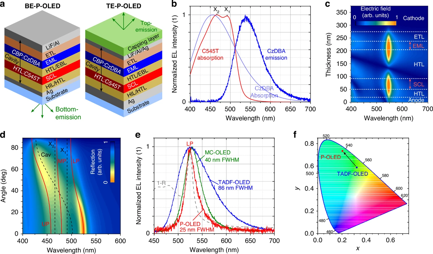
For that, both layers have to sit on an antinode of the cavity’s electric field. The team made the hole transport layer 140nm thick to raise the cavity to its second-order resonance, so that two field antinodes appeared.
The emitting layer went on one antinode and the C545T strong-coupling layer on the other. So that the thickened transport layer would not spoil charge balance, it was electrically doped with 4wt% F6TCNNQ.
4. A linewidth of 86nm narrowed to 25nm
This is what came out of comparing three devices side by side, all tuned to around 525nm. The reference TADF OLED had a full width at half maximum (FWHM) of 86nm, the microcavity OLED whose cavity was built with silver electrodes 40nm, and the polariton OLED carrying a strong-coupling layer 25nm.
The second half of that is this paper’s own share. The cavity alone narrows things as far as 40nm, and what took it from there to 25nm is the polariton. The reading is that the lower branch decays more slowly once light and exciton mix.
The change on the angle side is more striking. In the microcavity the emission peak was pushed 40nm toward the short side at 45 degrees. The device with a 20nm-thick strong-coupling layer gave 23nm, and the device whose cavity was made slightly thinner to pull the wavelength down gave 10nm.
The colour coordinates followed. The reference device’s broad green moved toward pure green, and the paper writes that the device tuned to 528nm comes close to the green primary set by the ultra-high-definition broadcast standard (BT.2020).
5. Putting in a thicker absorbing layer raised the efficiency
You would normally expect the opposite. Put a strongly absorbing layer inside the device, and make it thicker still, and it looks as though it should eat the light that ought to leave and spoil the outcoupling.
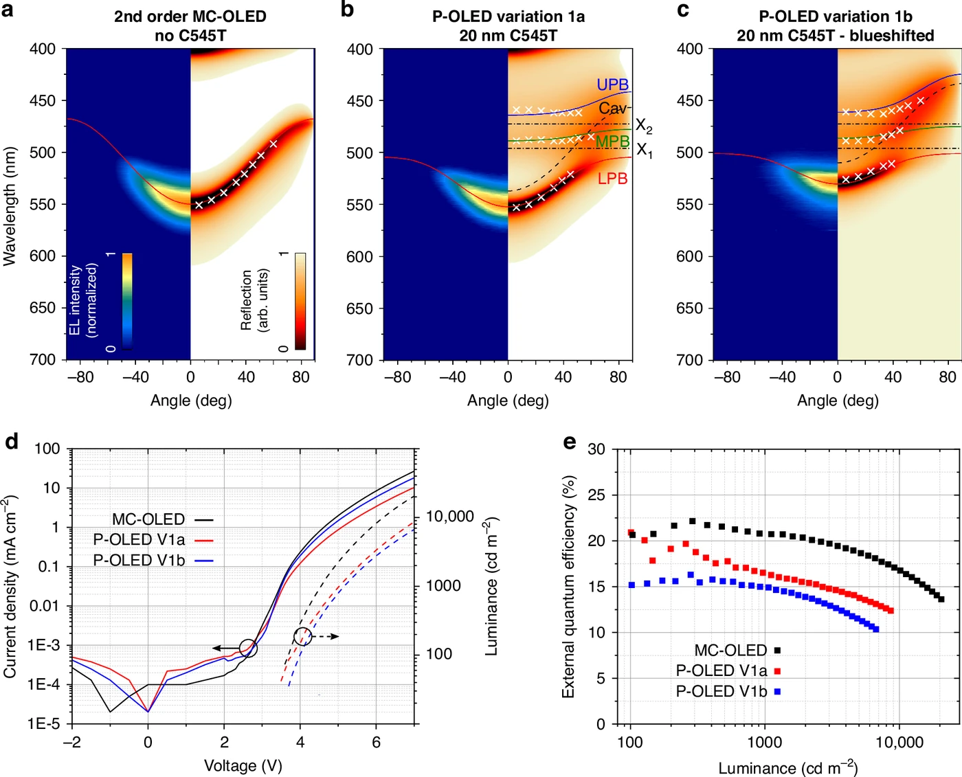
Yet thickening the C545T layer from 20nm to 40nm raised the efficiency. A device with an external quantum efficiency of 16.5% at 1,000cd/m² became 21.3%. That is the same level as the microcavity OLED with no strong-coupling layer (20.8%).
The reason the paper gives is the kernel of this work. Strong coupling itself is what keeps reabsorption away. The stronger the coupling, the further the emitting lower polariton branch is pushed toward low energy, away from the absorption peak of the strong-coupling layer.
Adding more absorber, in other words, is not a loss but a way of widening the gap between the absorption peak and the emission position. The Rabi splitting grew from 0.2eV to 0.4eV, and the colour shift at 45 degrees also fell slightly, from 23nm to 22nm.
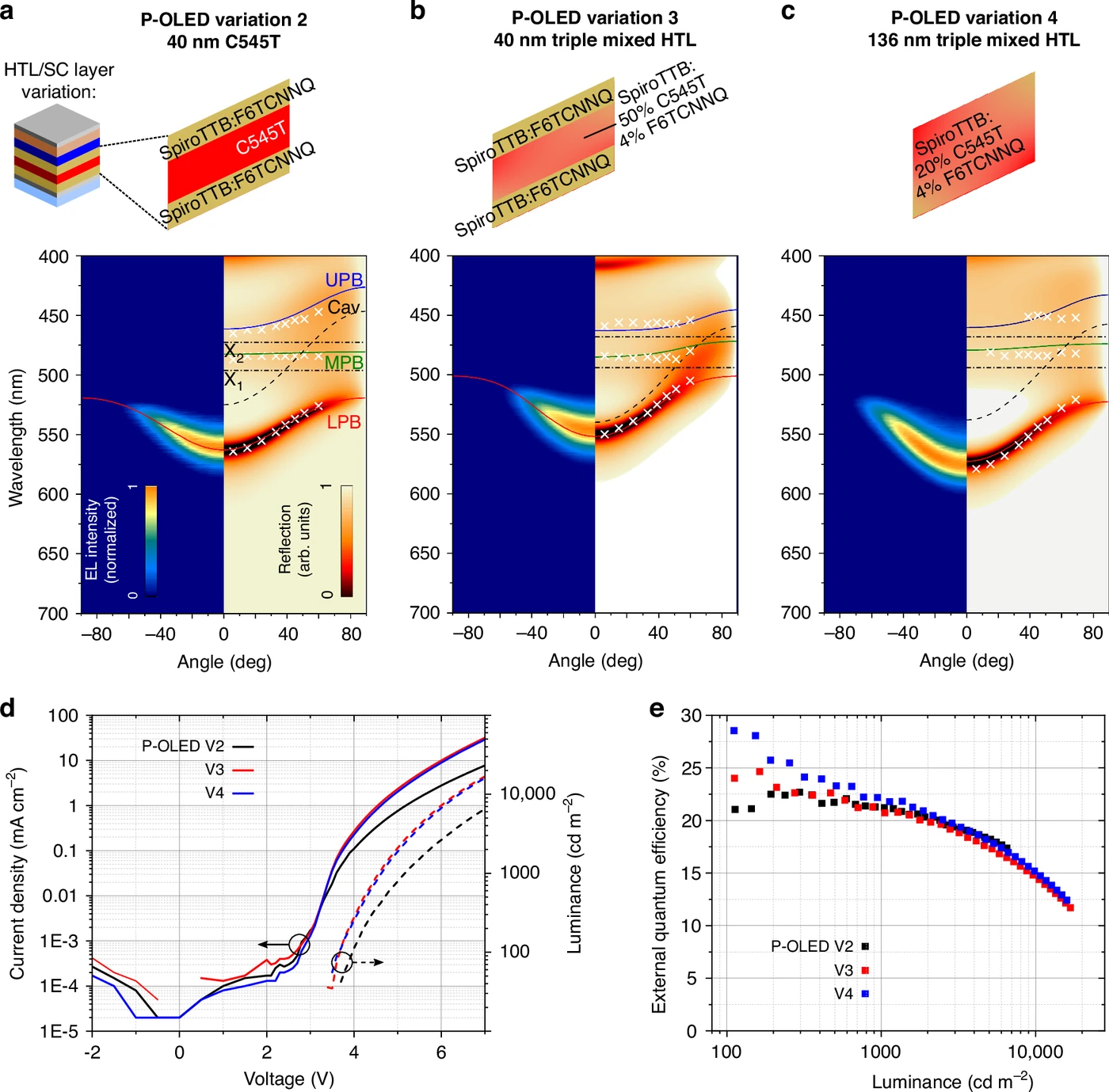
What remained was the electrical side. Put C545T in as a solid layer and holes have trouble getting through, so the current drops. At 6V the current density came down from the microcavity’s 8.4mA/cm² to 2.8mA/cm².
The team solved it by mixing the layer. They made a triple-mixed layer co-evaporating 50wt% C545T and 4wt% dopant into SpiroTTB, which carries holes well. Their grounds were that C545T’s HOMO lies deeper, so it does not become a hole trap.
In this device the current density came back to 9.9mA/cm², with 20.8% efficiency and a colour shift at 45 degrees of 22nm. The device that replaced the whole transport layer with a 136nm triple-mixed layer reached 22.0% at 1,000cd/m² and 28.6% at 100cd/m², the highest in this work.
6. It worked in a top-emitting structure too
The one displays actually use is top emission. Take the light out upward and the pixel circuitry stays uncovered, so the aperture ratio grows, and the stack can sit on an opaque substrate. Microdisplays built on a CMOS backplane are like that.
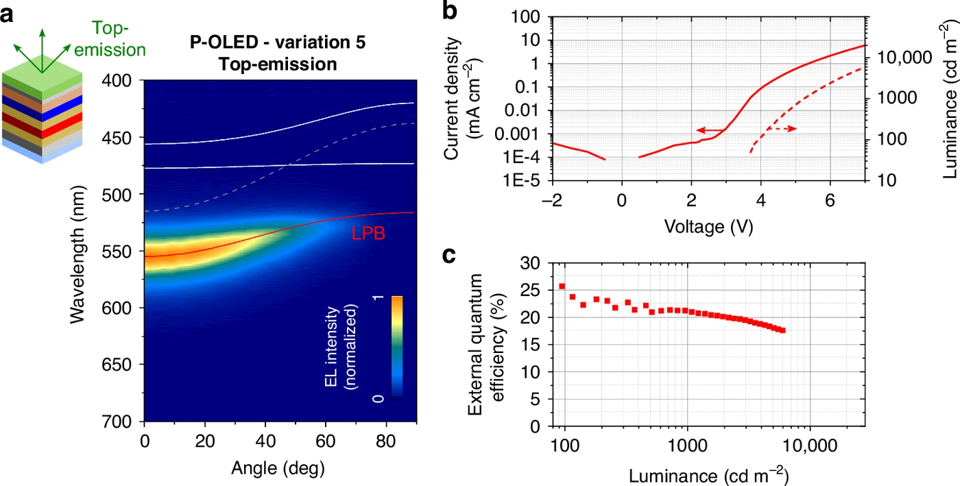
The team built a top-emitting polariton OLED with a thick silver reflector at the bottom, a thin semi-transparent silver electrode on top and a 60nm capping layer above that. Because it is a structure with no transparent conductive oxide electrode at all, the paper writes, it also avoids the damage that depositing such an electrode does to the organic layers.
The result was 555nm head-on emission, a 31nm FWHM, a 19nm colour shift at 45 degrees and 21.2% efficiency at 1,000cd/m². The device with the cavity pulled down to 541nm brought the colour shift as low as 10nm.
7. The trade that one table lays bare
No single device had all three. Copy the paper’s Table 1 across and you see it at once. The two best devices for colour shift, at 10nm at 45 degrees, sit at around 15% efficiency, while the most efficient device, at 22%, shifts by 29nm.
| Device | Head-on wavelength | FWHM | Colour shift at 45° | Efficiency (1,000cd/m²) | Current density (6V) |
|---|---|---|---|---|---|
| Microcavity | 550nm | 35nm | 40nm | 20.8% | 8.4mA/cm² |
| Polariton V1a | 550nm | 30nm | 23nm | 16.5% | 3.4mA/cm² |
| Polariton V1b | 528nm | 25nm | 10nm | 15.0% | 5.9mA/cm² |
| Polariton V2 | 560nm | 28nm | 22nm | 21.3% | 2.8mA/cm² |
| Polariton V3 | 546nm | 31nm | 22nm | 20.8% | 9.9mA/cm² |
| Polariton V4 | 573nm | 33nm | 29nm | 22.0% | 8.9mA/cm² |
| Top-emitting V5 | 555nm | 31nm | 19nm | 21.2% | 2.2mA/cm² |
| Top-emitting V5b | 541nm | 28nm | 10nm | 15.4% | 3.3mA/cm² |
Even so, the baseline moved up. Four of the polariton devices in the table passed 20% at 1,000cd/m², which the paper writes is more than double the best figure reported for earlier polariton OLEDs. It amounts to the first demonstration that a polariton structure does not cut efficiency badly.
There is also one place where something was gained without a trade. The triple-mixed-layer device (V3) matches the microcavity at 20.8% efficiency and 9.9mA/cm² current density, yet its colour shift halved from 40nm to 22nm and its linewidth narrowed from 35nm to 31nm.
The paper, rather than hiding this trade, concedes it in a line. Not every design presented here improved colour shift, linewidth and efficiency together, it writes in the discussion, and there may be an intrinsic trade-off among them.
8. Between the abstract and the body
There are four things to separate when reading this from the industry side.
First, the three words in the title are not one device’s score. “Narrowband, angle-stable, highly efficient” is a property of the whole family of devices this work covers. As the table in section 7 has it, the 10nm colour shift and the 21% efficiency came from different devices.
Second, it is one colour, green. The emitter used is a single green TADF material, and the strong-coupling layer a single green fluorescent dye. Whether the same combination works in blue and in red is not in this paper. What the paper states it is aiming at is the green pixel of ultra-high-definition displays.
Third, there are no lifetime data. The device area is 4mm², and what the paper carries is efficiency, current and angular characteristics. How the strong-coupling layer affects operational lifetime was not tested. Since the design puts an absorbing layer inside the pixel, that is the first item industry will ask about.
Fourth, “you only have to add one material” comes with conditions. The paper closes by saying that because the structure is almost the same as a conventional OLED and only one new material has to be added, commercial adoption should not take great effort.
But what actually changed is not one material. The premise is making the hole transport layer roughly 140nm thick and electrically doping it so that the cavity runs at second order. The best device replaced the transport layer itself with a three-material mixed film. One more evaporation source is needed, and the list of thickness and composition controls grows.
9. What remains for industry
That the job of purifying colour can be moved from the material to the optics is the point of this work. To get a narrow linewidth you normally redesign the emitting material itself. Multi-resonance TADF is that route, and quantum-dot colour conversion layers serve the same purpose.
The polariton does that job without changing the emitter. The paper offers it as an alternative to solutions that are expensive or raise toxicity concerns, and it did reach 25nm while keeping a donor-acceptor TADF emitter known for its broad linewidth.
That is also why working in top emission matters. A strongly reflecting metal electrode is the original cause of colour shift, yet this structure keeps that electrode and still gets colour consistency. Dropping the transparent conductive oxide, which makes the process more flexible, comes as a bonus.
The numbers that remain are 10nm and 15%. The device that tamed the colour shift best gave up the most efficiency. On the day those two meet in one device, it will be the cavity design, not the material, that decides the colour. What this paper showed is that the trade is no longer large.