
Reversible Photolithography Makes 21,000-PPI Quantum Dot Pixels
Turning quantum dots into pixels means locking their surface ligands together, and that locking is exactly what erodes device performance. Researchers at the Ningbo Institute of Materials Technology and Engineering, Chinese Academy of Sciences, built a ligand that a wavelength of light can lock and later unlock, restoring the surface after patterning is done. The result is 21,000 pixels per inch with an external quantum efficiency of 17.08%. Look at the tables side by side, though, and what patterning actually cut was not efficiency but current.
DOI 10.1038/s41467-026-77916-zTo use quantum dots as a screen’s pixels, they must stay only where they belong — red, green, and blue kept apart, each inside a cell just a few micrometers wide.
Semiconductor fabrication’s answer is photolithography. But putting photoresist on quantum dots degrades their performance. So the field turned to direct photopatterning, making the quantum dots themselves respond to light.
That runs into an old dilemma. For a pattern to survive, the ligands on the quantum dot surface have to be locked together, and that locking is what drags down device performance. The force that makes patterning possible and the force that erodes performance are one and the same.
Researchers at the Ningbo Institute of the Chinese Academy of Sciences made that locking reversible. A 310-nanometer UV wavelength locks it; a 254-nanometer deep-UV wavelength unlocks it. Once the pattern is finished, they simply unlock it again.
The result: an external quantum efficiency of 17.08% at 21,000 pixels per inch (0.8-micrometer pixel width), versus 24.41% and 125,016 cd/m² at 5V for an unpatterned device.
And what this article wants to flag is what comes next. Lay the tables side by side, and what patterning actually cut was not luminous efficiency but current.
1. Why printing quantum dots as pixels is hard
Because quantum dots wash away. Coat a substrate with quantum dots suspended in solution, and the solvent used in the next process step simply dissolves them right back off. So the quantum dots meant to stay put have to be locked to each other.
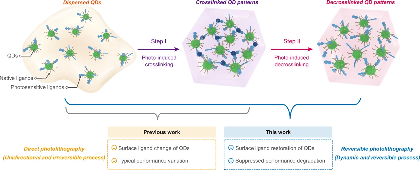
Direct photopatterning does that locking with light. Ligands in the illuminated area cross-link and stop dissolving in solvent; the unilluminated area washes away. Skipping photoresist keeps the process short.
The catch is what the ligand was already doing. A ligand caps defects on the quantum dot surface, sets the spacing to neighboring dots, and opens the path charge carriers travel. Decompose it, swap it, or lock it together, and all three change at once.
The paper calls this “an intrinsic coupling between patterning capability and performance degradation.” As it notes, quantum dot LEDs passed 20% external quantum efficiency long ago, yet devices that have gone through photopatterning typically fall below that.
2. A ligand that attaches and detaches by wavelength
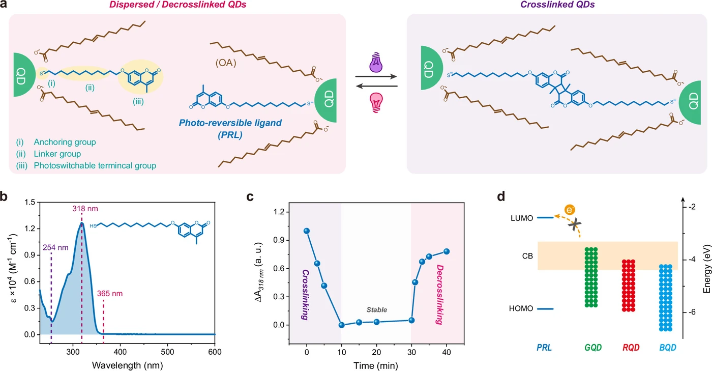
A molecule called coumarin attaches and detaches depending on wavelength. Under UV light longer than 300 nanometers, two coumarin molecules form a ring and bond; under deep UV shorter than 300 nanometers, that ring breaks apart again.
The researchers attached this property to a quantum dot ligand. One end carries coumarin, which bonds and unbonds with light; the opposite end carries a thiol group that binds tightly to the quantum dot surface; between them sits a long alkyl chain that keeps the molecule well dispersed in solvent.
There was a second reason to choose the thiol group. It bonds strongly with the zinc sulfide shell of the quantum dot, capping surface defects. Its calculated binding energy, at −1.19 eV, is deeper than oleic acid’s −0.75 eV.
This ligand’s LUMO sits at −2.41 eV, above the conduction bands of the red, green, and blue quantum dots (−4.00, −3.54, and −4.16 eV). Electrons have no path to leak into the ligand.
Among all the ligands on the quantum dot surface, this photoreversible ligand was optimal at about 8 mol%. Adding more preserved brightness but blurred the pattern edges.
3. A pattern forms at 5 mJ/cm² exposure
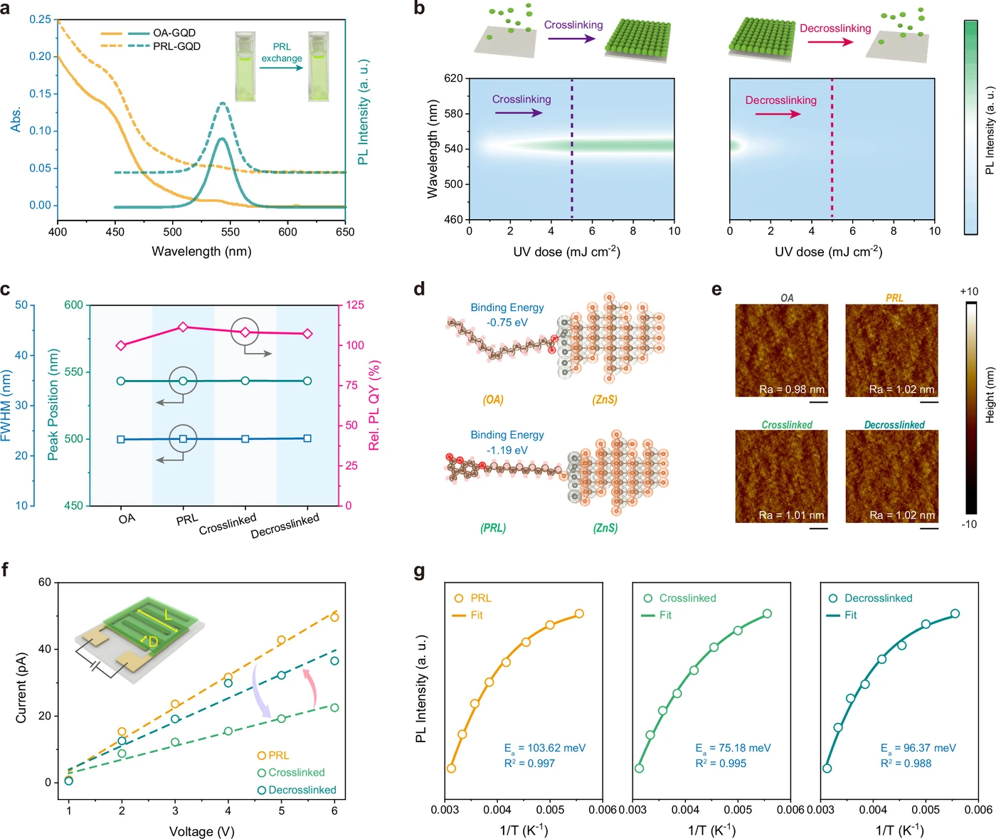
That’s about 1/20 the level of commercial photoresist. Films made with this ligand saturated in emission intensity around 5 millijoules per square centimeter. Commercial photoresist needs 80–150; semiconductor-grade photoresist needs over 200.
A lower exposure dose means the quantum dots take less UV damage. Areas left unexposed washed away completely after 10 seconds in toluene, giving sharp contrast.
Then comes this paper’s key number. After the full process cycle, the film’s relative photoluminescence quantum yield (PLQY) was 107.4% of the original quantum dots. The restored film ended up brighter than the untouched one — the thiol group’s contribution from capping surface defects.
The structure stayed nearly intact too. Surface roughness rose only from 0.98 nm to 1.02 nm, and the X-ray signal from the elements making up the quantum dot core didn’t change.
4. What did patterning actually cut?
Not efficiency — current. Line up a cross-linked device against an uncross-linked one, and that’s exactly what shows.
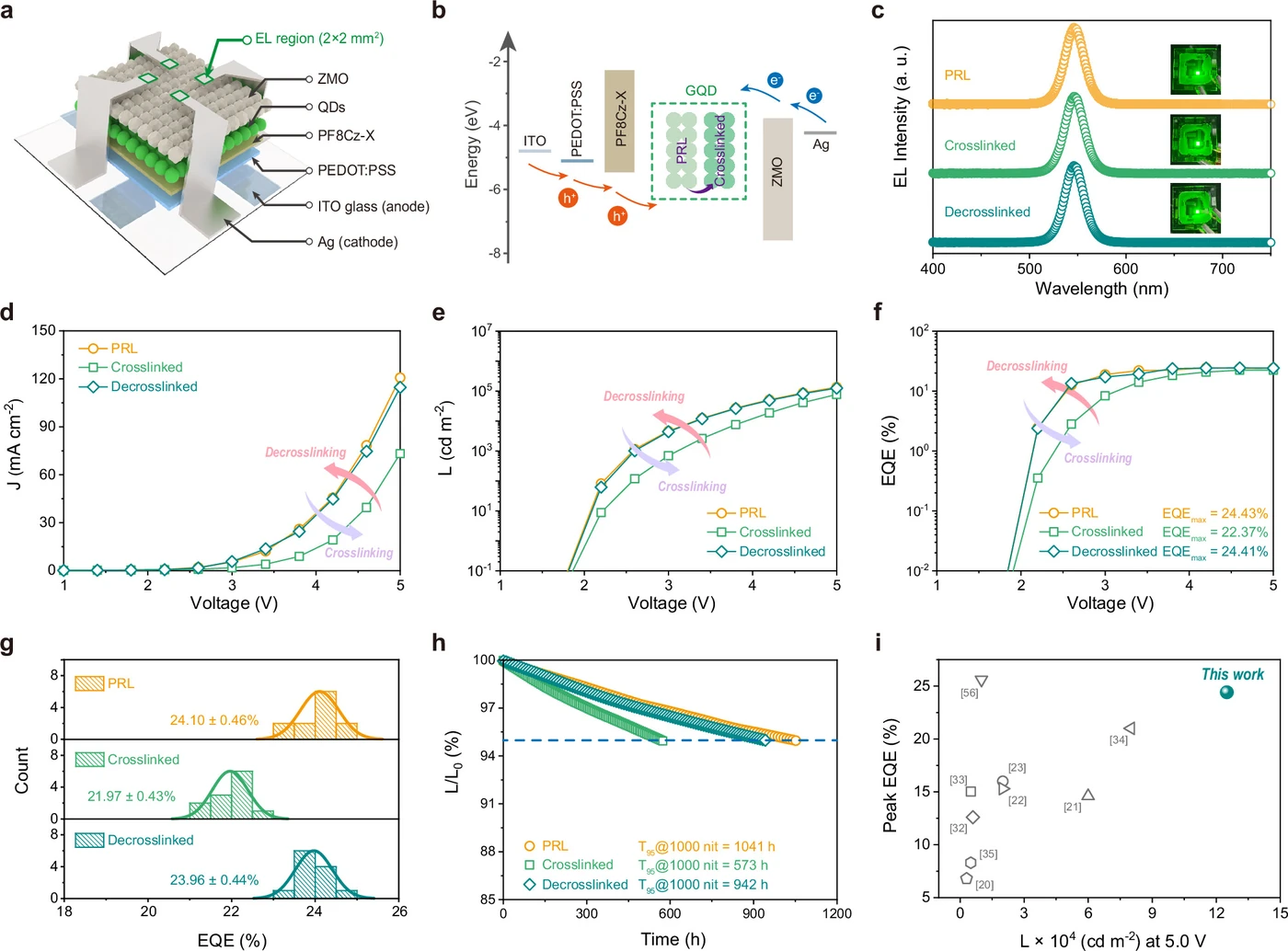
Peak external quantum efficiency fell from 24.43% to 22.37% — about an 8% drop. But at 5V, luminance fell from 134,796 to 76,632 cd/m², and current density from 120.7 to 73.2 mA/cm² — retaining only 57% and 61%, respectively.
In other words, the ability to convert charge into light barely moved, while charge simply stopped flowing well enough, cutting brightness roughly in half. The cause is spacing: the distance between quantum dots, measured by X-ray scattering, widened from 8.42 nm to 8.70 nm after cross-linking.
That’s 0.28 nanometers — about 3% of a quantum dot’s diameter — and it was enough to drag down conductivity. Current-voltage measurements on a lateral device also showed higher resistance in the cross-linked film.
The small efficiency drop has its own explanation too. The thermal activation energy, derived from temperature-dependent emission, fell from 103.62 meV to 75.18 meV. The researchers read this as a weakening of the force binding the exciton together. The efficiency gap was especially wide at low voltage (12.60% versus 2.82% at 2.6V).
And once the cross-links were broken, all three came back. Spacing, conductivity, and thermal activation energy (96.37 meV) all returned close to their original values.
5. Undoing the lock brought back the lifetime too
At 5V, luminance of 125,016 cd/m² and current density of 114.7 mA/cm² recovered to 93% and 95%, respectively. Peak external quantum efficiency reached 24.41% — essentially the same as before cross-linking (24.43%).
Averaged across 12 devices, the trend matches: 24.10±0.46% → 21.97±0.43% → 23.96±0.44%.
Lifetime tells the clearer story. Time to fall from an initial luminance of 1,000 nits to 95% dropped from 1,041 hours to 573 hours — cut roughly in half — then recovered to 942 hours after de-cross-linking.
What’s notable is the comparison against a device with the original ligand. An untouched oleic-acid quantum dot device reached 93,801 cd/m² at 5V and a peak efficiency of 23.53%. The device that switched to the photoreversible ligand, went through patterning, and was restored ended up both brighter and more efficient than that baseline. The value added by the ligand exchange — capping surface defects — outweighed the cost of patterning.
6. 17% efficiency at 21,000 PPI
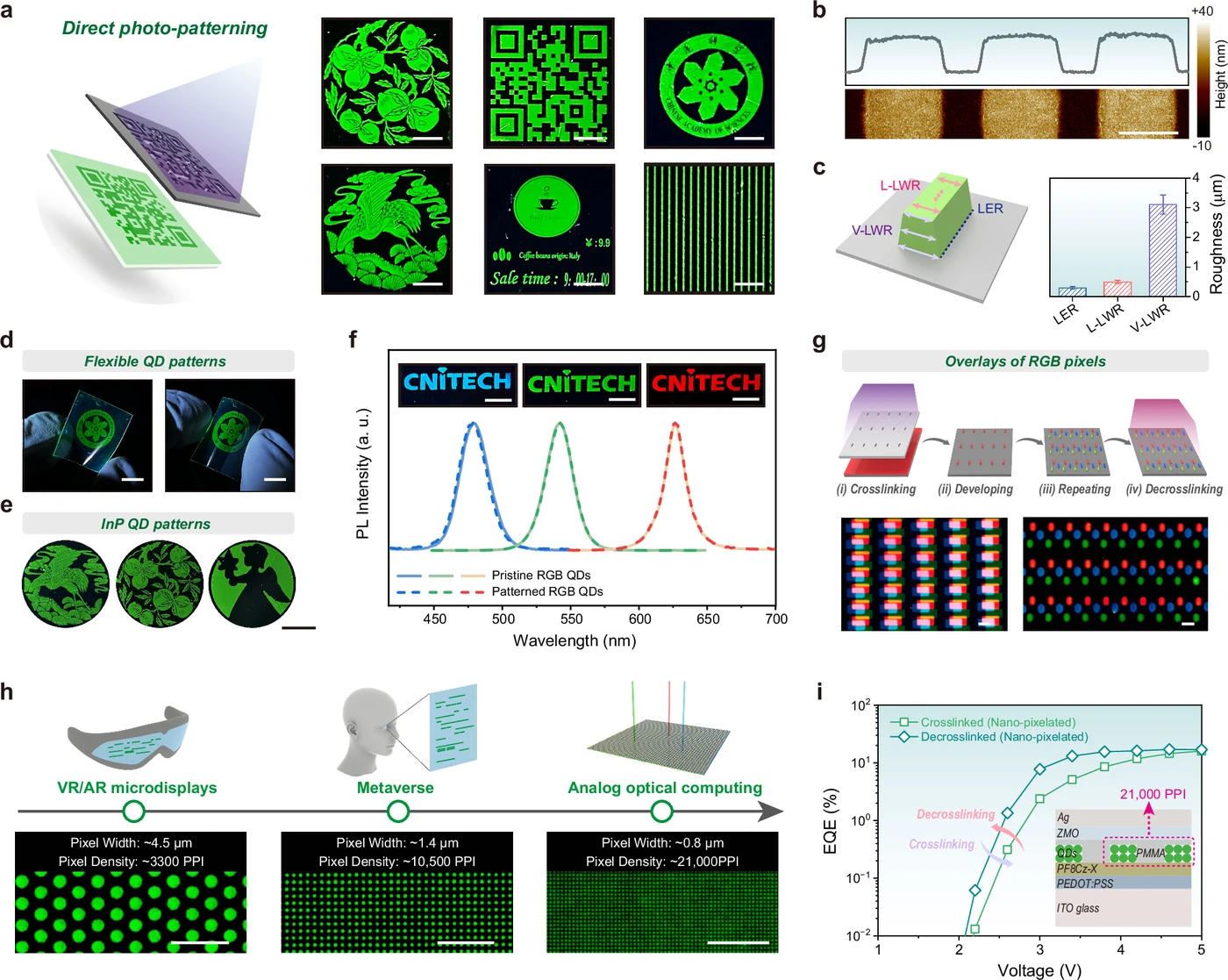
Pixel width 0.8 micrometers, pixel gap 0.41 micrometers, pitch 1.21 micrometers — equivalent to 21,000 pixels per inch. The paper describes this as among the highest resolutions reported for direct photopatterning.
Devices were built at three resolutions: 4.5-micrometer pixel width (3,300 PPI) for AR/VR, 1.4 micrometers (10,500 PPI) for higher density, and 0.8 micrometers (21,000 PPI), a resolution an order of magnitude beyond the eye’s resolving limit.
Dividing into pixels creates a new problem: in the empty space between pixels, the hole transport layer and electron transport layer touch directly, letting current leak through. The researchers plugged that gap with a thin coat of PMMA.
For the 21,000-PPI device, de-cross-linking raised luminance from 28,769 to 49,292 cd/m², current density from 40.7 to 65.6 mA/cm², and peak efficiency from 16.02% to 17.08% — still below the unpatterned device’s 24.41%.
The paper attributes the shortfall to three factors: the pixel shape isn’t ideal at this size, the pixel structure makes the electric field uneven, and residual PMMA hinders charge injection.
7. Between the abstract and the body
Five distinctions matter for reading this from an industry angle.
First, 24.41% and 17.08% are different devices. Of the two figures placed side by side in the abstract, the first is the value for an unpatterned 2×2 mm emitting area, and the second is the value for the actual pixel array. Luminance also differs by more than double, at 125,016 versus 49,292.
Second, the pixel array has no driving circuitry. These devices are structured as pixels arranged between blanket electrodes; the thin-film transistor or CMOS backplane needed to switch pixels individually is outside this paper’s scope. Using 21,000 PPI as an actual display would require a separate circuit capable of driving at that density.
Third, multicolor is not yet electroluminescence. The pixel array made by stacking red, green, and blue is a fluorescence image, produced by shining UV light on it. The electrically driven pixel array is green only. The paper itself describes multicolor integration as “a foundation for future work.”
Fourth, the restoration isn’t 100%. Luminance came back to 93%, current to 95%, lifetime to 90%. The paper attributes this to coumarin not breaking apart completely at 254 nanometers, settling instead into an equilibrium, and leaves it as something molecular design still needs to resolve further.
Fifth, values drop in air. The core experiments were run in a nitrogen glovebox. Running the same process in ambient air brings the photoreversible ligand’s luminous efficiency retention rate down to 83.3% — a consequence of shining UV light in the presence of water and oxygen.
8. What’s left for industry
What this research touched was not the material but the process. The quantum dots themselves are off-the-shelf cadmium-based core-shell particles, and the device structure is a known one. What changed is one ligand and two exposure wavelengths.
Methods for making quantum dot pixels split broadly into inkjet printing and photopatterning. Printing conserves material, but droplet size sets a floor on resolution. Photopatterning can go down to whatever resolution the mask defines, and this paper showed a way to keep performance intact at that resolution.
That it also works with cadmium-free InP quantum dots and on a flexible substrate matters for exactly that reason — both regulation and form factor are conditions real products actually demand. That said, in both cases the paper only demonstrated fluorescence patterns, not electroluminescence.
The numbers that remain are 0.28 nanometers and 93%. That much widening in the spacing between quantum dots cut brightness in half; undoing it brought back 93%. What this paper demonstrated, by building a process that can be reversed, is that what a quantum dot pixel process must protect is not the ability to emit light, but the distance charge has to cross.