The optical fingerprint sensor never sees your fingerprint
Ridges touch the cover glass and valleys do not. The 4.07 %p of reflectance that difference creates is the entire contrast of a fingerprint image — drawing a picture with 4 out of 100. There is no separate light source either, so OLED pixels are the illumination, and with no room to stand an imaging lens, angle has to be cut away with apertures. Raising resolving power fourfold means throwing away 15 times the light.
This article was published before the English edition began, so the labels inside its figures and simulators are in Korean. The caption and the note under each figure are in English.
1. The screen is the illumination
Press a finger down and that spot brightens for a moment. Anyone who uses a phone sees it several times a day. It is easy to take for a marker showing where to press. It is not.
That light is this sensor’s light source.
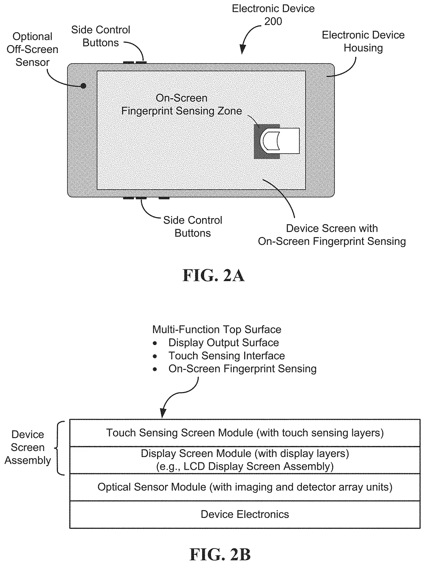
An optical fingerprint sensor under the screen has no illumination of its own. It turns on OLED pixels to light the finger, and an image sensor under the panel reads the light that comes back. The brightening is not a marker but an exposure. What happens on the screen is the same thing as a flash firing when the shutter is pressed.
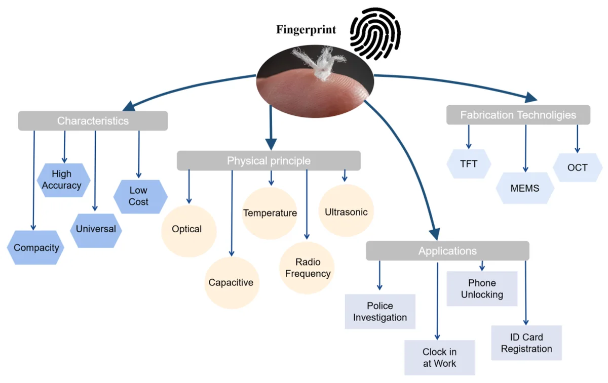
Every constraint on this approach follows from that one fact. If the illumination is the screen, its colour cannot be chosen freely, the whole panel sits between illumination and subject, and above all there is no thickness in which to stand an imaging lens. This article follows those constraints one at a time.
This series has been about why putting a sensor under the screen becomes a different problem for each sensor. The camera’s image was blurred by diffraction, the proximity sensor’s signal fell as the square of the round-trip transmittance, and the ambient light sensor was fooled by light the screen itself emitted. The fingerprint sensor is the first of them to go under the screen, because its subject is pressed against the glass and the distance is close to nothing.
The date is 2017. Synaptics announced Clear ID FS9500 in 2017-12, and the Vivo X20 Plus UD carrying it appeared in early 2018. For that same year Goodix writes in its own corporate history that it “launched the world’s first optical in-display fingerprint sensor.”1 The two companies’ claims overlap, so this article does not decide who was first. What is clear is what came next. Goodix states that it commercialized the approach broadly in 2018 and mass-produced an ultra-thin product in 2019, and it holds under-display optical fingerprint patents on the scale of thousands. The place that first laid out the principle and the place that made the volume are different. Operating systems began treating this sensor as a formal category considerably later, from Android 12, when the name UDFPS for an under-display fingerprint sensor entered the documentation.2
2. What separates ridge from valley is the contact surface
What the sensor reads is not a fingerprint but a map of reflectance. The only thing making that map is whether the finger touches the glass or not.
Ridges touch the cover glass. The interface there is glass and skin. Valleys do not. The interface there is glass and air. The two interfaces differ in refractive index contrast, so they return light differently.
| Interface | Refractive index | Normal-incidence reflectance | Critical angle |
|---|---|---|---|
| glass and air (valley) | 1.51 / 1.000 | 4.13 % | 41.5 degrees |
| glass and water (wet valley) | 1.51 / 1.333 | 0.39 % | 62.0 degrees |
| glass and skin (ridge) | 1.51 / 1.440 | 0.06 % | 72.5 degrees |
On a dry hand the reflectance difference between valley and ridge is 4.07 %p. That value is the entire contrast of the fingerprint image. It amounts to drawing a picture with 4 out of 100.
The size of the pattern to be read is fixed too. Ridge width is 100 to 400µm, valley width 75 to 200µm, valley depth 60 to 220µm.3 Taking one ridge plus one valley as a period of 200µm gives five cycles per millimetre. That is the spatial frequency the sensor has to resolve.
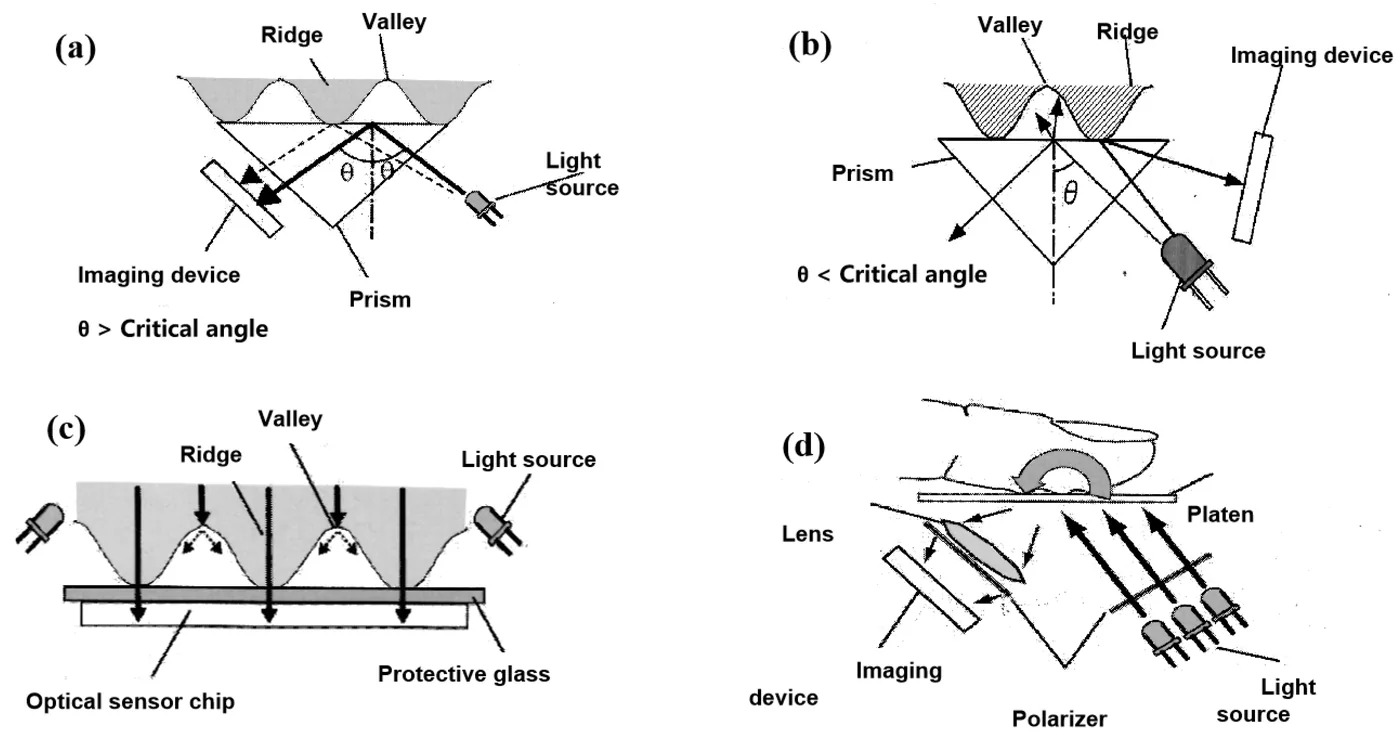
Raise the angle and contrast explodes
The 4.07 %p used so far is the value for light striking the interface normally. Strike it obliquely and the story changes completely.
Going from a medium of higher refractive index to one of lower, beyond a certain angle not a scrap of light crosses over and all of it returns. That is the critical angle. Glass to air is 41.5 degrees, glass to skin 72.5 degrees. In the range between them valleys return everything while ridges leak almost all of it away.
Work it out and the contrast between 41.5 and 72.5 degrees is 97.5 %p. Against the 4.07 %p near normal incidence that is 24 times. This is why (a) and (b) in the figure above go to the trouble of using total internal reflection. It makes contrast 97 out of 100 rather than 4 out of 100.
Push the angle toward 41.5 degrees and the valley curve rises like a cliff to 100%. Fill the valley with water and that cliff is pushed out to 62.0 degrees. The contrast that lay between 41.5 and 62.0 degrees vanishes wholesale. How the optical approach weakens on a wet hand is explained entirely by that cliff moving.
The grey band is the range of angles the collimator lets through. The range where contrast explodes lies outside that band. What that mismatch means comes back in Section 4.
Strictly speaking, skin is not a mirror but a scatterer. A real signal includes not only surface reflection but backscatter from light that enters the skin and returns. The reflectances given in this article are normal-incidence Fresnel values, to be read as a baseline for how large a problem the contrast is.
3. There is no thickness in which to stand an imaging lens
In a camera you would put a lens here. A lens gathers light from one point on the finger onto one point on the sensor. That correspondence is what forms an image.
Under the screen there is no room for it. From cover glass through panel to sensor is around a millimetre, and no imaging optics can be stood in that gap. What happens without an imaging lens? Light from every point on the finger reaches every pixel of the sensor. Each pixel ends up seeing the whole finger, and the image becomes a uniform grey.
So a different method is used. Instead of gathering, it discards.
Deep, narrow holes are cut in the path of the light, letting through only rays arriving almost normally and killing oblique rays against the walls. That angle-filtering layer is the collimator. A Synaptics patent sets out the layer order directly.
Below the input surface are display elements that emit light, below that an aperture layer, below that a collimator layer, and below that again light-sensing elements.4
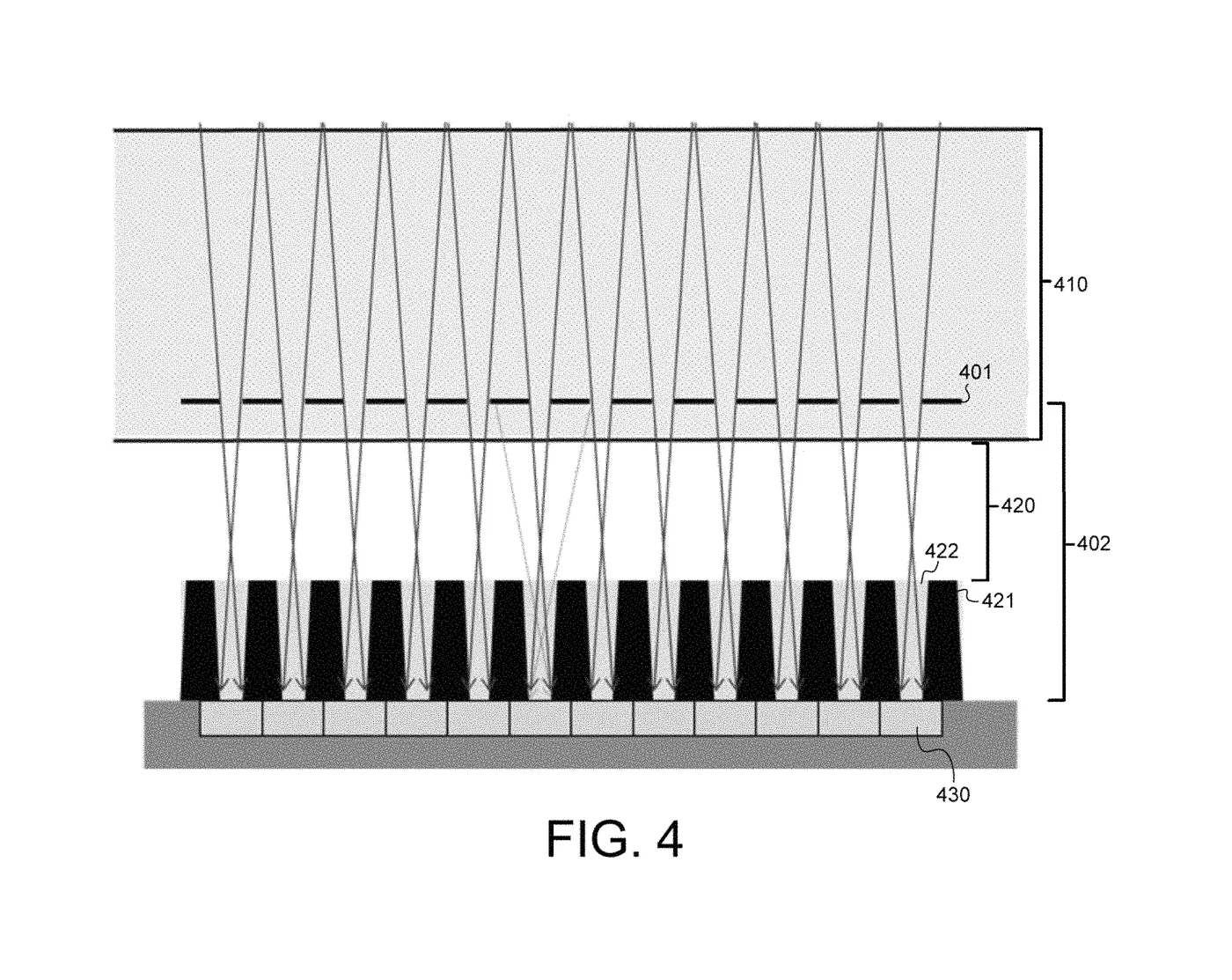
Another patent from the same company sets out why. The apertures and reflective surfaces “limit the angle of light reaching each light-sensing element so that the light reaching that element corresponds to a relatively small region of the object.”5 Angle limiting takes over the job an imaging lens used to do. The microlenses that come later are not a substitute for that job; they are collectors that pick up light the apertures discarded.
One design variable falls out here. The depth of the hole divided by its width, the aspect ratio. The review cited above names precisely this as an advantage of the under-display structure: the value can be chosen freely.3
4. The narrower it gets, the sharper and darker at once
Raise the aspect ratio and the maximum acceptance angle narrows. In a hole whose width to depth is 1 to 10, only light with a slope gentler than 0.1 gets through.
The maximum acceptance angle is the arctangent of the reciprocal of the aspect ratio. An aspect ratio of 10 gives 5.71 degrees, 20 gives 2.86 degrees. That angle settles two things at once.
First, the area one pixel sees. With a cover thickness h, light from within a diameter of 2h·tanθ mixes into one pixel. That diameter is the blur.
Second, the amount of light received. As the collection solid angle narrows, light falls roughly in proportion to sin²θ.
Setting cover thickness at 0.6 millimetres, it works out like this.
| Aspect ratio | Max acceptance angle | Diameter a pixel sees | Relative light collected |
|---|---|---|---|
| 3 | 18.43 degrees | 400 µm | 10.0 % |
| 5 | 11.31 degrees | 240 µm | 3.85 % |
| 10 | 5.71 degrees | 120 µm | 0.99 % |
| 20 | 2.86 degrees | 60 µm | 0.25 % |
| 30 | 1.91 degrees | 40 µm | 0.11 % |
Raise the aspect ratio from 5 to 20 and the blur goes from 240µm to 60µm, four times sharper, while the incoming light falls by a factor of 15.4. The price of four times the resolving power is 15 times the light. That is the essence of this approach, and the rest of the design is entirely about how to pay that trade less painfully.
A baseline can be calculated too. To resolve a ridge period of 200µm the blur has to stay under half of it, 100µm. On a 0.6 millimetre cover that condition means an aspect ratio of 12 or more. With a hole of aspect ratio 5, a fingerprint looks like a grey smear.
But a fingerprint holds something smaller than ridges. Sweat pores, lined up along the ridge crests. The review puts sweat pores first when it enumerates the features of a fingerprint.3 At a pore the skin does not touch the glass, so optically it is the same interface as a valley, and it registers as a bright dot on a dark ridge. Taking the diameter as 60µm, the condition for keeping them is an aspect ratio of 20.
How far down you want to read is how far up you push the aspect ratio, and that value is how much light you throw away. An aspect ratio of 12 suffices for ridges alone, but sweat pores need 20, and between the two the light falls fourfold again.
Push the aspect ratio from one end of its range to the other and the ridges come alive from a grey smear into a pattern, and past 20 sweat pores appear dotted along them. In exchange the picture turns grainy, because as light falls the noise grows relatively larger.
Push the contact state toward dry and a completely different kind of collapse appears. On a dry hand the hardened outer skin lifts the ridges minutely off the glass. It is not that some ridges touch and others do not; the fraction of area actually in contact falls across the board. The reflectance there lands somewhere between the skin value and the air value, and the difference from the valleys shrinks accordingly.
Work it out and as the contact area falls from 95% to 16% the contrast falls from 3.87 %p to 0.65 %p, a sixfold drop. On screen it looks like this. You can tell the whorl is there, but you cannot follow individual ridges. It is not smeared and it is not erased; the signal is simply not there. There is no blur to restore, only something that was never captured, and for the side extracting and matching minutiae there is nothing to be done. This is why collimation performance in real sensors is measured as signal-to-noise ratio. The review cited above records that improving collimation technology raised the signal-to-noise ratio by nearly a factor of two.3
Blur scales directly with cover thickness too. Fix the aspect ratio at 10 and change only the thickness: 0.3 millimetres gives 60µm, 1.5 millimetres gives 300µm. Once the cover gets thicker, the same hole cannot give the same picture. That is why sensitivity design for in-cell fingerprint sensors using thick cover glass becomes a conference topic of its own.6
Overlay the angle story from Section 2 here and one more layer of what this approach pays comes into view. The contrast between 0 and 5.7 degrees that the collimator passes does not budge from around 4.07 %p however far the aspect ratio is raised. Narrowing the aperture reduces blur; it cannot increase contrast. And the 97.5 %p that total internal reflection creates is out of reach entirely.
The under-display optical approach starts by giving up the angles where contrast is largest. With no room for a prism, there is no choice. The attempt to win those angles back is the configuration in Section 6 that uses the cover glass itself as a waveguide.
This trade belongs to the same family as the ones earlier in this series. In the under-display camera episode, the more you opened the space between pixels to let in more light, the worse the diffraction and the blurrier the image. Here, the narrower the hole, the sharper the image and the more the light disappears. Only the direction differs; the fact that touching the aperture moves brightness and sharpness in opposite directions is the same.
5. Industry solved thickness by folding it
Raising the aspect ratio needs a deep hole, and depth needs thickness. But under the screen there is no thickness. How that contradiction is resolved splits by company.
Fold the light. Synaptics folded the optical path by combining apertures with reflective surfaces. In the patent’s phrasing, a “folded collimator minimizes the thickness of the detection section within the display.”5 Light going down, reflecting back up and down again buys a path length several times the actual thickness.
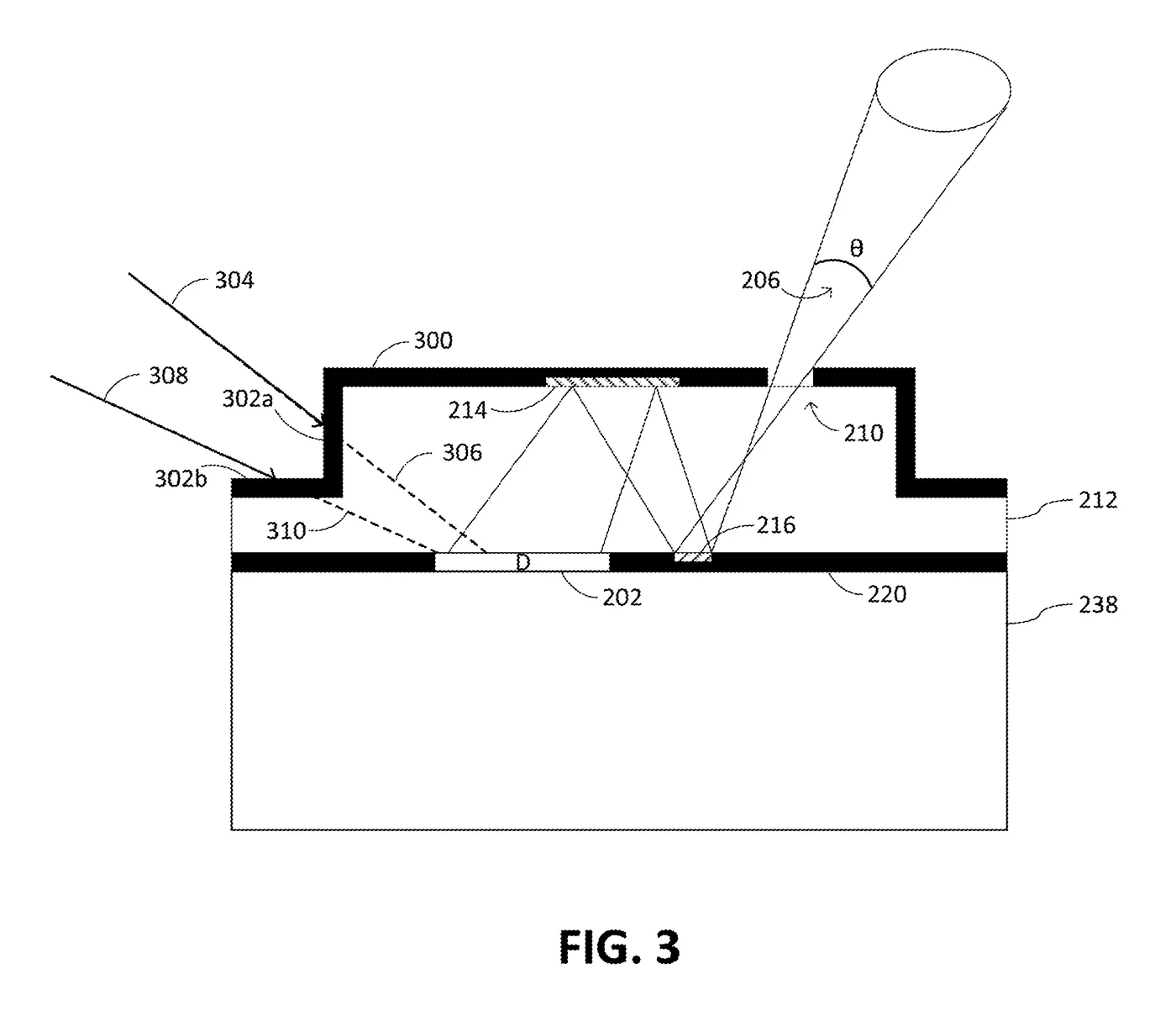
Lay the lens and pinhole on their side. Goodix claimed a structure tilting the optical axis between 45 and 135 degrees from the sensor surface normal, with the pinhole placed off the optical axis.7 Another patent folds the path by bouncing light between two mirrors.8 In both cases, thickness that cannot be stacked vertically is secured by laying it out horizontally.
Make up for it with microlenses. Cutting angle with holes alone only discards light, but putting a small lens over the hole gathers some of what would be discarded. It is not an imaging lens forming a picture but a collecting lens funnelling light into the aperture. In the configuration the review sets out, a 940nm infrared source and a microlens array were combined, with angles designed so that oblique light undergoes total internal reflection at the upper and lower faces of the cover glass.3
All three branches solve the same problem: cut the angle but discard less light.
6. The rest of the homework, all because the illumination is the screen
Thickness is not the only problem. That the illumination is the screen exacts a price elsewhere too.
The colour cannot be chosen. OLED pixels emit only in red, green and blue. Reflection and scattering in skin depend on wavelength, so which colour illuminates changes image quality. A Synaptics patent separately claims a scheme that illuminates alternately with the red and the green subpixel and uses the difference.4 Unable to make the illumination it wants, it works the illumination it has.
Using infrared means a light source of its own. Near-infrared penetrates skin more deeply and is less shaken by surface contamination. But OLED pixels do not emit near-infrared. Hence configurations that place a 940nm source separately under the cover, or lay organic photodiodes on oxide TFTs to tile near-infrared sensing pixels at a 50.8µm pitch for 500 PPI.3
Use the cover glass itself as the light source. Another Synaptics patent attaches a layer of lower refractive index beneath the cover glass to trap light inside it.9 The glass becomes a waveguide, and the signal appears where the finger touches and the confinement breaks. It is a way of making illumination without turning the screen on, an attempt to do away with the screen brightening every time a fingerprint is read. The separate infrared source above points the same way.
Even the assumption that it is OLED-only wavers. The optical approach is commonly explained as working only on self-emissive OLED, since the screen has to give off light. Yet Goodix separately claimed an optical fingerprint module placed beneath an LCD screen.10 It uses the backlight or a separate source as illumination and tiles a photosensor array under the panel. In the patent landscape at least, it is not OLED-only.
7. The real weak point is not a wet hand but a dry one
That the optical approach is weak to water falls straight out of the arithmetic. Fill the valley with water and the interface becomes glass and water, dropping reflectance from 4.13% to 0.39%. The difference from the ridge falls from 4.07 %p to 0.33 %p, a more than 12-fold cut. The critical angle is pushed from 41.5 to 62.0 degrees as well, shaving even the margin that total internal reflection had banked.
And yet what the literature names first as the optical approach’s weakness is not a wet hand.
Optical under-display fingerprint sensors use the difference in light reflected from ridges and valleys, and have difficulty distinguishing a dry finger, because it does not contact the cover layer regularly and consistently.3
On a dry hand the hardened outer skin keeps the ridges from touching the glass evenly. A ridge that does not touch looks like a valley to the sensor. The pattern is not erased; it is turned into the wrong pattern. If a wet hand lowers contrast, a dry hand scrambles it.
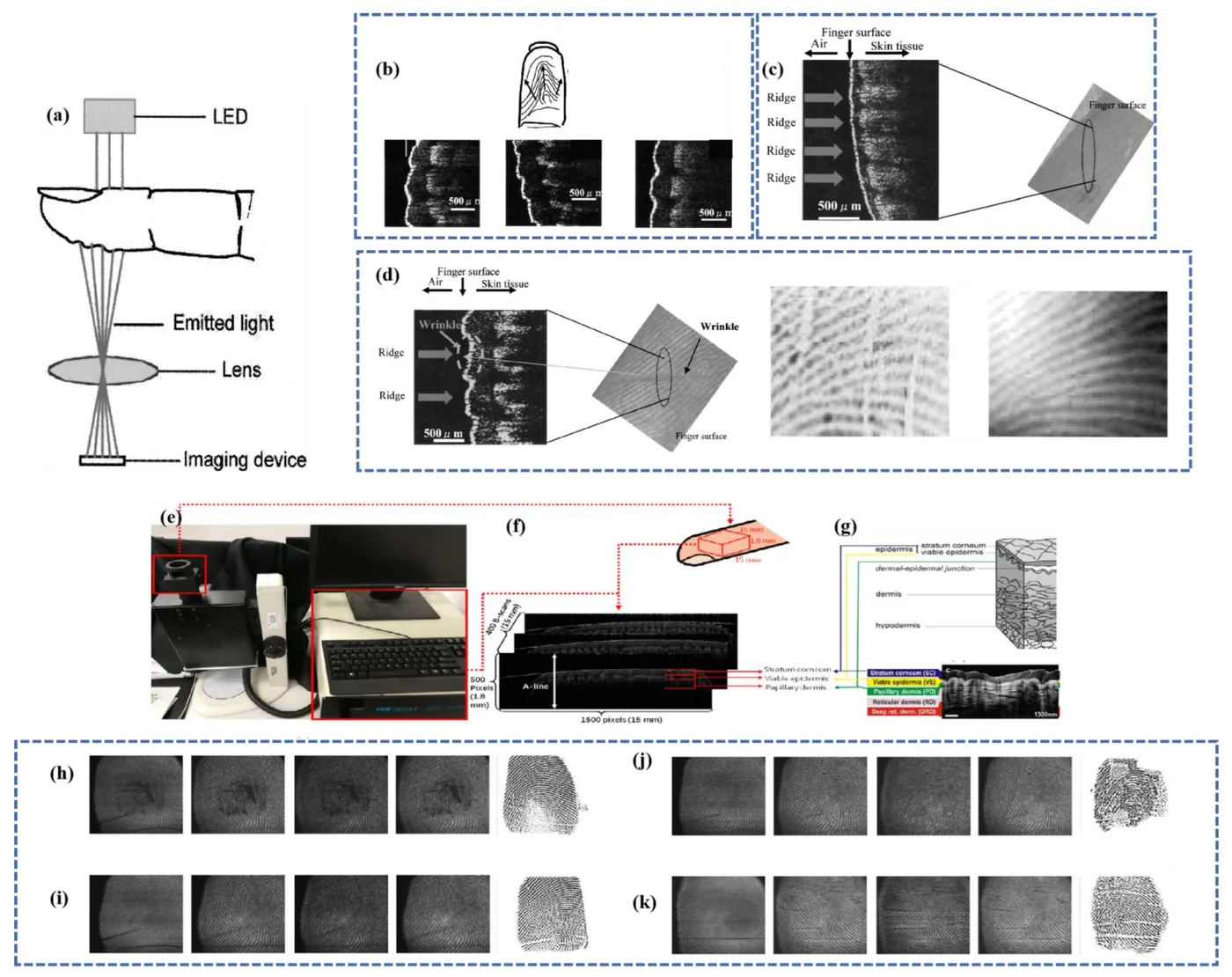
The two are opposite ends of the same cause. What this approach reads is not the finger but the boundary between finger and glass, and the direction in which that boundary is disturbed is all that separates water from dryness. The physical structure of the fingerprint is intact in both cases. The sensor simply cannot reach it.
The security problem arises in the same place. The optical approach sees only the surface. If the light-and-dark pattern of the surface matches, there is little in the optical signal to tell whether it belongs to a living finger or a printout. Hence separate discrimination of forged patterns follows in the patents,11 and devices appear that use spectroscopy to confirm whether it is real skin.12 They are traces of the industry conceding that the optical signal alone is not enough.
Certification standards treat the optical approach separately
This is not conjecture; it is written into the standard.
Android divides biometric implementations into three classes. To go beyond screen unlock into app authentication and the keystore requires the highest, Class 3, whose requirements are a spoof acceptance rate (SAR) at or below 7%, a false acceptance rate (FAR) of 1 in 50,000, and a false rejection rate (FRR) of 10%.2 Spoof acceptance rate is a metric newly introduced in Android 9, measuring how well a sensor withstands an attack in which a forgery is actually made and presented to it.
And the test specification sets recommended spoof materials separately for each sensor type. That list confirms this article’s argument directly.
| Sensor type | Spoof materials the standard recommends |
|---|---|
| optical | non-conductive ink on copy paper or transparency film, gelatin, latex paint, wood glue |
| capacitive | gelatin, wood glue, latex paint |
| ultrasonic | gelatin, wood glue, latex paint |
Paper appears only for the optical type. The test procedure splits as well. The optical type is told to use both flat and three-dimensional forgeries, while capacitive and ultrasonic have only the procedure of making a three-dimensional mould from a lifted print. The judgement that a flat printout can work against an approach that reads only surface light and shade is written into the standard itself.
The test conditions are demanding too. Rather than the subject cooperating to have a mould taken of their finger, the forgery must be made the uncooperative way, from a print left on another surface. Exactly as a real attacker would.
One threshold moves two errors in opposite directions
Of those three figures, spoof acceptance rate can only be measured by actually making and presenting a forgery, so set it aside; the other two are different in character. False acceptance and false rejection are two ends of the same handle.
Authentication scores how closely the enrolled features and the features just read resemble each other, and unlocks when that score passes a threshold. Another person’s finger happening to score high is a false acceptance; the owner’s finger scoring low is a false rejection. Raise the threshold and the first falls while the second rises. The same structure as raising the aspect ratio to sharpen the image while losing light.
The trouble is that everything this article has followed so far flows into this point. When contrast is low and the image is blurred, the distributions of other people’s scores and the owner’s scores overlap. To the extent that they overlap, no threshold placement can satisfy both requirements together.
Call the separation between the two distributions, in standard deviations, the separability. The arithmetic comes out as follows. The threshold that meets a false acceptance rate of 1 in 50,000 sits at 4.11 standard deviations in the impostor distribution. For the false rejection rate at that threshold to be under 10%, the separability must be 5.39 or more.
| Separability | False rejection rate when false acceptance is met |
|---|---|
| 4.0 | 54.3 % |
| 5.0 | 18.6 % |
| 5.39 | 10.0 % |
| 6.0 | 2.9 % |
Fall short of a separability of 5.39 and no threshold whatsoever reaches Class 3. Lower the threshold and false acceptance leaves the requirement; raise it and false rejection does.
Drop the separability below 5.39 and push the threshold to either extreme and the green indicator never comes on. What optical performance ultimately decides is that one screen.
To clear this threshold the optical approach fetches evidence from outside the optical signal. It illuminates alternately in two colours and compares the responses,7 or checks whether it is real skin from the difference in penetration depth by wavelength,12 or learns forged patterns themselves and filters them out.11 Because a single 4 %p image, made by cutting angle with a collimator, cannot carry that demand.
The two weaknesses — being shaken by contact state, and seeing only the surface — share a root. It reads the boundary with light. So what happens if the boundary is read with something else? A way of reading the same finger with sound rather than light is already in phones, and that is the next and final episode of this series.
8. Key terms
- collimator
- A layer that arrays deep, narrow holes to filter out obliquely arriving light and pass only near-normal light. It stands in for an imaging lens where none can be stood.
- aspect ratio
- The depth of a hole divided by its width. The larger it is, the narrower the range of angles passed, so the image sharpens and the brightness falls.
- Fresnel reflection
- The phenomenon in which part of the light returns at a boundary between two media of different refractive index. The larger the index contrast, the more returns.
- critical angle
- Going from a medium of higher refractive index to one of lower, the boundary angle beyond which all light returns.
- in-cell
- Building the sensor into the display panel itself rather than attaching it as a separate component.
- spatial frequency
- How dense a pattern is, expressed as cycles per unit length. A fingerprint is around five cycles per millimetre.
Footnotes
-
Goodix Technology (603160.SH) corporate profile history. The 2017 entry reads “Launched the world’s first optical IN-DISPLAY FINGERPRINT SENSOR,” the 2018 entry broad commercialization, and the 2019 entry the world’s first mass production of an ultra-thin product. It is material a listed company disclosed to investors, and Synaptics introduced its own product as a first in the same period. This article does not adjudicate which was first. ↩
-
Android Open Source Project, “Measure biometric unlock security.” The requirement table by class, the fingerprint authentication evaluation procedure and the list of recommended spoof materials by sensor type are in this document. The formal name of the spoof acceptance rate is Impostor Attack Presentation Match Rate, and the fingerprint baseline was set at 7% in Android 9. The same document also states that Class 2 covers a spoof acceptance rate of 7 to 20%, and that Class 3 must fall back to primary authentication after at most 72 hours. ↩ ↩2
-
Y. Yu et al., “A Review of Fingerprint Sensors: Mechanism, Characteristics, and Applications,” Micromachines 14(6), 1253 (2023). A joint review by the School of Optoelectronic Engineering at Xi’an Technological University and BOE Display Technology, organizing more than 250 references. The ridge and valley dimensions, the depth-to-width ratio of the apertures, the dry finger problem, the signal-to-noise improvement, the 940nm microlens configuration and the oxide TFT based 500 PPI configuration are all descriptions from this source. ↩ ↩2 ↩3 ↩4 ↩5 ↩6 ↩7
-
US10268884B2 (Synaptics Inc.), “Optical fingerprint sensor under a display.” The quoted layer structure and the alternating red-green subpixel illumination are taken from the claims and embodiment descriptions. ↩ ↩2
-
US10169630B2 (Synaptics Inc.), “Optical sensor for integration over a display backplane.” The quotation is the patent’s own wording. ↩ ↩2
-
C.-C. Lai et al., “39-1: Designing high-sensitivity optical sensor for in-cell fingerprint sensor with thick cover glass in OLED display,” SID Symposium Digest 54(1) 554-557 (2023). Only the problem framing its title points to is cited here; the figures in the paper body were not confirmed. ↩
-
US10824838B2 (Shenzhen Goodix Technology), “Under-screen optical fingerprint sensor based on lens-pinhole imaging with an off-axis pinhole.” ↩ ↩2
-
US20200034602A1 (Shenzhen Goodix Technology), “Optical fingerprint sensor with folded light path.” ↩
-
US20190138154A1 (Synaptics Inc.), “Systems and methods for injecting light into cover glass.” It claims a configuration placing an inner layer of lower refractive index in direct contact beneath the cover glass. ↩
-
US10410033B2 (Shenzhen Goodix Technology), “Under-LCD screen optical sensor module for on-screen fingerprint sensing.” The review cited above writes that the optical and ultrasonic approaches are compatible only with OLED panels, but this patent and the review’s own LCD in-cell description run against that. ↩
-
US10318791B2 (Shenzhen Goodix Technology), “Anti-spoofing sensing for rejecting fake fingerprint patterns in under-screen optical sensor module.” ↩ ↩2
-
CN112183483A (Egis Technology), “Integrated real finger spectrum sensing device and sensing method.” ↩ ↩2