The ultrasonic fingerprint sensor is stopped by the adhesive, not the glass
Acoustic impedance is the geometric mean of density and stiffness. Glass and adhesive differ by a factor of 2.2 in density but by 34 in stiffness, so their impedances part by 8.6 times. Crossing 700 micrometres of cover glass loses essentially nothing, while a single 20-micrometre adhesive layer beneath it drops one-way transmission to 9 %. Industry has only two routes: make it so thin it might as well not be there, or dope it with particles to raise its stiffness.
This article was published before the English edition began, so the labels inside its figures and simulators are in Korean. The caption and the note under each figure are in English.
1. What happens inside 233 nanoseconds
That there is a fingerprint sensor under the screen is no longer a remarkable story. But look at that spot a little closer and one thing is strange.
A whole sheet of glass sits between the sensor and the finger.
A flagship’s cover glass is generally around 0.7 millimetres, with the encapsulation and pixel layers stacked below it. The finger is on top of that glass and the sensor is underneath. An optical sensor turns on screen pixels to fire light and looks at what comes back. That was the previous episode. The ultrasonic type does not use light. It fires sound into the glass.
In numbers it looks like this. The speed of sound in soda-lime glass is 6,000 metres per second. A round trip through 0.7 millimetres takes 233 nanoseconds. One of four million slices of a second. The time a person feels between touching a finger and the lock opening is a little over 0.2 seconds, but the unit of time in which the physics happens inside it is six orders of magnitude away from that.
This article follows those 233 nanoseconds in five stages. Make the sound, fire it, get it back, choose when to look, and read it. Four of the five are places this series has not yet covered, and the real design decisions of this sensor are in those four.
First, one incident that tells us exactly what this method reads.
In October 2019 it was reported that unregistered fingerprints could unlock the Galaxy S10 and Note10. The cause was physical before it was a software bug. The three-dimensional pattern on the surface of certain silicone protective covers was read by the sensor as a fingerprint, and enrolling a fingerprint with that cover on mixed the cover’s pattern into the enrolled data. Samsung Electronics acknowledged the problem and distributed a software patch, advising users not to use those covers until patched and, after patching, to re-enrol their fingerprints with the protective film removed.
The sensor did not look at the finger; it read an acoustic map of the screen surface. The cover’s pattern was there, so that is what it read. There is no clearer illustration of what this method reads.
2. Making the sound
For there to be sound coming back, sound has to be made first. This is the first place the ultrasonic type parts from the optical. The optical type borrows the screen’s pixels as illumination. The ultrasonic type carries its own signal source.
That source is the piezoelectric layer. Qualcomm’s large-area module patent describes the operation like this.
“an applied transmitter excitation voltage changes the thickness of the piezoelectric transmitter layer 422, and in that manner generates ultrasound at the frequency of the transmitter excitation voltage” (US10891458B2)
Apply a voltage and the layer thickens and thins. That vibration becomes sound directly. There is no lens and no focus. It is a plane wave, the whole surface pushing at once. This is where its character parts completely from the earlier episodes on the camera and Face ID. There the question was which direction the light came from; here it is when the sound arrived.
The same patent specifies materials and thicknesses.
| Item | Value |
|---|---|
| transmit piezo layer | PVDF about 28µm |
| receive piezo layer | PVDF-TrFE about 12µm |
| general range | 5-30µm, narrowly 5-15µm |
| other materials listed | PVDC · PTFE · DIPAB · AlN · PZT · sodium bismuth titanate |
| frequency | 1-100MHz, practically 5-20MHz |
A polymer was chosen over materials an order of magnitude more sensitive
Here is the strange part. PVDF is not among the better performing piezoelectric materials. Place the measured values from Onda’s acoustic properties tables side by side and the difference is plain.
| Material | Speed [km/s] | Density [g/cm³] | Acoustic impedance [MRayl] | Q |
|---|---|---|---|---|
| PVDF | 2.30 | 1.79 | 4.2 | 10 |
| PZT-5H | 4.44 | 7.43 | 33.0 | high |
The 2023 review goes as far as a device-level comparison. A PZT-based sensor structure has an order of magnitude higher radiation sensitivity than a 110 × 56 PMUT-based sensor and two orders higher than a CMUT-based one. In integrated sensitivity too, PZT-5 based was the highest among the designs compared.
And yet what went under the screen is the PVDF family. The same review puts the reason in one sentence.
“unlike piezoelectric ceramics such as PZT, P(VDF-TrFE) films are CMOS compatible and can be integrated directly with the supporting electronics”
Process compatibility. PZT is a ceramic needing high-temperature sintering, so it cannot go straight onto a TFT backplane or CMOS. The PVDF family is a polymer film that can be coated and poled at low temperature and laid directly on readout circuitry. It was not chosen for winning a piezoelectric coefficient contest but for being able to get inside display and semiconductor processes.
This is the first reason a display publication has to cover this sensor. It means the sensor’s material was set not by piezoelectric coefficient but by backplane process.
The same logic repeats in another lineage. The review names AlN as the early material of the PMUT family. AlN too has a lower piezoelectric coefficient than PZT, and was used for the process advantages of being lead-free and depositable at low temperature. Two independent lineages each chose a material weaker than PZT, and in both cases the reason is process.
Where a low Q is actually a gain
There is one more value in the properties table to watch. PVDF’s Q is 10. A low mechanical quality factor means that once struck, it stops quickly. Strike a bell and it rings a long time; strike a wooden board and it goes thud. PVDF is the board.
Thinking only of sensitivity, this is another drawback. In this sensor it is a gain. A short ring means a short pulse, and a short pulse is what lets depth be separated. This value returns in Section 5. For now it is enough to note that sensitivity was not the only thing looked at in choosing the material.
The same character of trade is in the thickness. The resonant frequency of the thickness vibration mode is the speed of sound divided by twice the thickness. Calculated at PVDF’s speed of 2,300m/s it comes out like this.
| Thickness | Thickness resonance |
|---|---|
| 5µm | 230 MHz |
| 12µm | 96 MHz |
| 28µm | 41 MHz |
| 30µm | 38 MHz |
The resonance of the 28-micrometre transmit layer is 41MHz while actual operation is 5-20MHz. It is used far below resonance. Used at resonance the sensitivity is maximal but the bandwidth is narrow. Narrow bandwidth means a long pulse, and a long pulse again means depth cannot be separated. Working in the flat region below resonance is standard practice for a broadband transducer, and here too the trade of selling sensitivity to buy bandwidth appears once more.
3. Firing it
How is the sound made sent out? The drive signal is not a continuous wave but a tone burst, a short slice of vibration at a set frequency. If the time of return is to be measured, the time of transmission has to be sharp, so this is the obvious choice.
The problem is area. For something the size of one finger, the whole layer can be rung at once. But the large-area cases the patent gives are 30 × 20 millimetres, 60 × 40 millimetres, and 70 × 150 millimetres. The last is the whole screen. Ringing an area like that at once is beyond the power budget.
So the electrodes are divided into segments. Only the region where the finger sits is driven, and two arrangements are presented: long continuous stripes and separate islands. Power certainly falls. There is a price, though, which the patent states directly: the gaps between segments create distortion and discontinuity in the image.
Here a side talent of this structure emerges. The electrode segments can be used, undriven, as a passive piezoelectric microphone array. A finger touching the screen creates a faint vibration of its own, which is picked up and read as low-resolution touch. It serves to check whether a finger is there before imaging the fingerprint. The same layer is both speaker and microphone.
Large area has walls of another kind too. The patent explicitly names the problem of large-area glass substrates cracking during lamination and says it is unfavourable for yield. Making the whole screen a fingerprint sensor is blocked by process before physics.
Two layers, front and back
The piezoelectric layer alone does not send sound out properly. Two more layers attach, front and back.
The backing layer handles the sound that goes backward. The piezoelectric layer vibrates both ways, so sound going back, left alone, returns from the substrate and enters the sensor late. Mixed with the real signal from the front, it ruins the image. Among the patent’s implementations is one making the second transmit electrode thick, copper at 100 micrometres, so it serves as both electrode and backing, and another placing a separate high-impedance non-conductive acoustic layer of density 3,500-10,000 kg/m³. It is a design separating the electrical role (a thin conductive layer) from the acoustic role (a thick dense layer).
The matching layer helps the sound going forward. Insert a layer of intermediate value between two media of greatly differing impedance and reflection falls. What that intermediate value should be comes from calculation. The 2020 review of acoustic matching for piezoelectric transducers states the standard conclusion: transmission is maximal at the geometric mean of the two impedances. The geometric mean of glass at 13.44 and tissue at 1.5 is 4.49 MRayl.
How the patent hits that value is interesting. Epoxy is doped with particles to change its density, and changing density changes acoustic impedance. The optimum the calculation gives is what industry matches with a mixing ratio.
4. Getting it back
Now the sound crosses the glass and reaches the finger. How much comes back has to differ from place to place for there to be a pattern.
The contrast impedance makes
The previous episode looked at where the contrast of an optical fingerprint sensor comes from. Ridges touch the cover glass and air stays in the valleys. The refractive index differences of glass to air and glass to skin differ, so the reflectance at the two places parts. That difference was 4.07%p. It amounted to drawing a picture with 4 out of 100.
For sound, acoustic impedance takes the place of refractive index. It is density times speed of sound, and expresses how heavy the medium feels to the sound. What returns at a boundary is set by a formula of exactly the same shape as for light.
R = ((Z₂ - Z₁) / (Z₂ + Z₁))²
The 2023 review puts the acoustic impedance of the air in a valley at 430 Rayl and that of human tissue, the ridge, at about 1.5 MRayl. A factor of 3,500. In refractive index that same place was air at 1.000 and skin at 1.44, a factor of 1.4. Calculating the normal-incidence reflectance seen from the cover glass (13.44 MRayl) gives this.
| What is on the finger side | Ultrasonic reflectance | Optical reflectance |
|---|---|---|
| valley (air) | 99.99% | 4.13% |
| ridge (skin) | 63.87% | 0.06% |
| difference, ridge to valley | 36.12%p | 4.07%p |
Read with sound, the contrast is nine times larger. It is also independent of screen brightness. That the screen does not flash in the dark, and that it can work with the screen off, both follow from this method making its own signal, as seen in Section 2.
Another Qualcomm patent specifies even the direction. At a ridge the acoustic impedance rises and the reflected amplitude falls accordingly (US10438040B2). The 63.87% and 99.99% in the table above are exactly that relation. It is why ridges come out dark and valleys bright in a fingerprint image.
One place where the sources disagree
At this point a disagreement between sources was found. Section 5 of the 2023 review cited repeatedly above contains this sentence.
“because of the acoustic impedance difference between human tissue and air, the echo amplitude of human tissue is larger than the echo amplitude of air”
This statement has the direction reversed. Air has a far larger impedance difference from glass and sends back 99.99%, while tissue sends back only 63.87%. The valley’s echo is larger. It contradicts the Qualcomm patent quoted in the paragraph above and the table’s own calculation.
It is an open-access review with 48 citations, so an easy place to copy across. This article followed the patent originals and the calculation. Not to disparage the review, but because a publication that lists all its sources should, on principle, state what it chose when the sources disagree.
There is more than one way to read
Everything so far reads the magnitude of the returning sound. The review calls this pulse-echo imaging, and says there is one more method.
“there are two main imaging techniques: pulse-echo imaging and impedance imaging”
Impedance imaging does not look at the echo. It rings the transducer and looks at how quickly the ringing dies away. In the review’s phrasing, it measures the attenuation in the contact area from the ring drop of the pulse.
The principle is this. Where a ridge touches, vibration energy leaks away into the finger so the ringing stops quickly. In a valley with only air there is nowhere to go, so it rings on. The rate of decay is the contact. The physics making the contrast is the same impedance difference, while the quantity measured changes from amplitude to time.
There is one more thing that can be read. The review cites a CMUT waveguide method measuring a phase difference of 0.6 degrees between ridge and valley at 2.4MHz. Amplitude, attenuation and phase all become information.
5. Choosing when to look
This section is the most important place in the article.
It seems one could simply take all the returning sound, but no. Plenty arrives besides what came from the finger. The wave reflected at the surface reaches the sensor side, bounces back up and returns a second and a third time. It rings inside the glass. Sound that passed through the finger surface returns from boundaries inside the skin and arrives later.
So this sensor cuts by time. Qualcomm’s imaging patent specifies the numbers.
“the acquisition time delay may be in the range of about 10 nanoseconds to about 20,000 nanoseconds or more. In some implementations the first acquisition time window may be in the range of 5 to 50 nanoseconds” (US11017251B2)
The same patent also states what those two values set. The time delay is matched to the expected time of return by reflection from the platen surface; the first delay and window make the image correspond to fingerprint features, and the second delay and window make it correspond to subdermal features.
In short there are two handles to work: when to start looking (time delay) and how long to look (time window).
Attach the values calculated earlier and the size of these numbers becomes tangible.
| Value | |
|---|---|
| round trip through 0.7mm glass | 233 ns |
| round trip through 1.0mm glass | 333 ns |
| one period at 10MHz | 100 ns |
| one period at 20MHz | 50 ns |
| surface fingerprint time window | 5-50 ns |
The upper end of the surface window equals one period at 20MHz, and the lower end is 1/10 of a period. It means the returning waveform is not received whole to inspect its shape; a value at a particular instant is sampled. Where that instant is placed decides what is seen.
The defaults are a 0.7 millimetre cover, a delay of 233 nanoseconds and a window of 50 nanoseconds. The window catches the moment the surface echo arrives and the verdict says it is looking at the fingerprint on the surface. Push “when to start looking” toward 750 nanoseconds and widen the window to 300 nanoseconds and the same sensor starts looking below the epidermis. The patent on harmonic detection specifies that region as 0 to 7.5 microseconds after the waveform peak (US10410034B2).
Here the Q from Section 2 returns
Change the piezoelectric material in the simulator to PZT and the picture collapses wholesale. The peak spreads wide and the verdict changes. The pulse is too long, and surface and dermis overlap on the time axis.
The reason comes from calculation. The ringing time is roughly Q divided by frequency, and half the distance the sound travels in that time is the depth that can be separated.
| Material | Q | Ringing time at 20MHz | Separable depth |
|---|---|---|---|
| PVDF | 10 | 500 ns | 385 µm |
| PZT family | 80 | 4,000 ns | 3,080 µm |
Taking the epidermis as 400 micrometres thick, the gap between surface echo and dermal echo is 519 nanoseconds. PVDF’s 500 nanoseconds just fits inside it; PZT’s 4,000 nanoseconds is over eight times too long. Three millimetres is close to the thickness of a finger. With a pulse like that there is no way to separate surface from subsurface in time.
Section 2 said PVDF was chosen over PZT, an order of magnitude more sensitive, and gave process compatibility as the reason. That is the first reason. Here is the second. What was bought by giving up sensitivity is time resolution. A material that rings hard rings long, and long ringing disarms this sensor’s central device, the time window.
Where the optical collimator used to be
In the previous episode the optical fingerprint sensor cut incidence angle with a collimator. Narrowing the aperture discarded light leaking in from neighbouring pixels, at the cost of darkness.
The ultrasonic type does the same job with time.
| Optical (episode 5) | Ultrasonic | |
|---|---|---|
| What is filtered | light arriving at the wrong angle | sound arriving at the wrong time |
| Tool | collimator aperture | acquisition time delay and window |
| Price | it gets darker | the energy received falls |
| How to adjust | the structure has to change | only the values change |
The last row matters. A collimator cannot be changed once made, while a time window is changed in software. The same hardware looks at the fingerprint and then, by moving the window, under the skin. Section 8 shows how this property becomes a feature.
6. Reading it
When the returning vibration shakes the piezoelectric layer, charge appears on its surface. That charge has to be read pixel by pixel to become an image. Qualcomm’s multi-functional sensor patent sets out the circuit directly.
“each sensor pixel 1934 may be associated with a local region of piezoelectric sensor material (PSM), a pixel input electrode 1937, a peak detection diode (D1) and a readout transistor (M3), with many or all of these elements formed on or in the substrate to constitute the pixel circuit 1936” (US10438040B2)
The sequence of operation follows. When the piezoelectric material converts the received ultrasonic energy into charge, the peak detection diode D1 holds the maximum charge detected. Each row of the pixel array is then scanned through a row select mechanism, gate driver or shift register, and the readout transistor M3 turns on column by column so that pixel’s peak charge is read out through a multiplexer and an A/D converter.
In one line it goes like this.
returning ultrasound → piezo layer converts to charge → pixel input electrode
→ peak detection diode D1 holds the maximum
→ gate driver scans the row → readout transistor M3
→ multiplexer → A/D conversion
Row select, gate driver, shift register, column readout. To anyone on the display side this list is not unfamiliar. It is the same as driving a TFT array. Indeed the same patent lists silicon, SOI, TFT substrate, glass, plastic and ceramic side by side as sensor substrates, and describes the circuitry on the substrate as “TFT circuitry on a TFT substrate or CMOS circuitry on a silicon substrate.”
The pixel listens to sound instead of emitting light. The structure is the same. Section 2 said the material was decided by the backplane process; the readout structure came from the same place. This is why this sensor is an object of the display industry.
What D1 does is worth another look. Holding the maximum means throwing away the time information and keeping only the magnitude. When it arrived has already been handled by the time window of Section 5. The instant is fixed by the moment the window opens, and the pixel remembers only the size of what came inside it. Two devices divide the roles between them.
7. When it cannot be read
That was the case where it works. Now the case where it does not. And the reason it does not comes from the very number that made the contrast large in Section 4.
The other face of the same number
A large impedance difference means large contrast and at the same time that the boundary is hard to cross.
The acoustic impedance ratio of glass to air is more than 30,000. The share of sound going from glass into air is 0.013%. The other 99.99% comes back. That is the same number that gave a contrast of 36.12%p.
The trouble is that this wall stands almost regardless of the thickness of the air layer. Even with a ridge touching the glass, if a very thin film of air remains in between, the sound returns before it meets skin. Check it with a single-layer transmission line calculation and it goes like this.
| Air left under the ridge | Ultrasound share reaching skin | Light share reaching skin |
|---|---|---|
| none (full contact) | 36.13% | 99.94% |
| 10nm | 1.07% | 99.74% |
| 50nm | 0.04% | 95.53% |
| 100nm | 0.011% | 88.39% |
| 1µm | 0.0001% | passes, effectively |
A single gap of 10 nanometres drops the signal from 36% to 1%. That is one ten-thousandth the width of a hair, and at that same spot 99.7% of the light passes straight through.
The two results part because of the impedance ratio. To light, 10 nanometres is 1/55 of a 550-nanometre wavelength, effectively nothing. To sound, 10 nanometres is also far thinner than a wavelength, but the impedance ratio is so large that being thin does not help.
This tells us what the real weakness of the ultrasonic type is. Not a wet hand but a dry one.
A finger with hardened, stiff outer skin does not bring the whole ridge into even contact even when pressed against glass. Wherever it does not make contact becomes, in that instant, exactly the same interface as a valley. When ridges look like valleys, the fingerprint is not a pattern but a smear. Indeed dry finger recognition is named alongside recognition time and manufacturing yield as a problem to improve for ultrasonic under-display sensors.
Conversely, a little moisture on the fingertip fills those minute gaps. Water’s acoustic impedance of 1.494 MRayl is essentially the same as skin’s, so to sound a place filled with water is indistinguishable from skin. The contact is completed. This is the physical substance of the claim that the ultrasonic type is strong with wet hands. Not because water helps the signal but because water pushes out the air.
If that moisture fills the valleys as well, though, it inverts. With water in the valley, valley reflectance falls from 99.99% to 63.99%, only 0.12%p from the ridge’s 63.87%. The contrast collapses to 1/300. That is why the review qualifies its statement about wet hands with “can be identified even with a small amount of dust or moisture.”
The culprit is not the film but the air under it
Put a protective film on the screen and one more layer appears between cover glass and finger. Intuitively, another layer means less signal. The calculation is not that simple, because the ultrasonic wavelength is the same order as the film thickness. At 10MHz the wavelength in PET is 254 micrometres and commercial films are generally 100 to 300 micrometres. Reflections travelling within the layer interfere with each other.
Apply the matching layer logic from Section 3 as it stands and the result comes out rather differently from intuition.
| State on the screen | One-way transmission | Round-trip transmission |
|---|---|---|
| no film (direct contact) | 36.1% | 13.1% |
| tempered glass film 300µm, full contact | 36.1% | 13.1% |
| PET film 100µm, full contact | 46.4% | 21.5% |
| PET film 63µm (quarter wave), full contact | 85.3% | 72.8% |
| 10nm air under the film | 1.07% | 0.011% |
| 1µm air under the film | 0.0001% | 0% |
This table is a lossless upper bound, without the share of sound absorbed inside the layers. Real values are lower, and how much lower is looked at separately at the end of this section.
Three things emerge at once.
First, a fully contacted tempered glass film is acoustically transparent. Tempered glass has the same acoustic impedance as the cover glass, so from the sound’s point of view there is no boundary at all. The glass simply got a little thicker.
Second, a well-chosen film actually raises the signal. Set PET to a quarter-wave thickness and one-way transmission goes from 36% to 85%. The film is not an obstacle but the matching layer from Section 3. The review’s remark that a 1-micrometre aluminium oxide protective layer has “almost no effect on sound transmission” is another region of the same calculation.
Third, one air layer ends everything. Neither material nor thickness matters. Choose the tempered glass perfectly and if a 1-micrometre bubble is left underneath, the signal is zero.
So the claim that a film stops fingerprint recognition is only half right. Precisely, there must be no air left between film and screen. That is why so-called fingerprint-compatible films manage adhesive method and thickness separately, and why the outcome rests on the fingertips of whoever applies them.
Select tempered glass and raise the “air left under the film” slider by just 10 nanometres and the curve sticks to the floor. Conversely select PET and set the thickness near 63 micrometres and it rises above direct contact.
There are layers under the glass too
All of that is above the glass: finger, air, protective film. But this sensor’s stack has layers beneath the glass too, and that side is more awkward.
First the materials have to be organized. Section 4 introduced acoustic impedance as density times speed of sound, and since the speed of sound itself comes from the material’s stiffness, one more step can be taken. The longitudinal speed is c = √(M/ρ) where M is the elastic modulus in that direction, the longitudinal modulus. Combine the two and impedance resolves into two material properties.
Z = ρc = √(ρ·M)
The geometric mean of density and stiffness. Why this form is needed is visible as soon as the numbers are laid out.
| Material | Density kg/m³ | Longitudinal speed m/s | Longitudinal modulus M | Impedance Z |
|---|---|---|---|---|
| soda-lime glass | 2,240 | 6,000 | 80.6 GPa | 13.44 MRayl |
| acrylic | 1,190 | 2,750 | 9.0 GPa | 3.27 |
| PET | 1,180 | 2,540 | 7.6 GPa | 3.00 |
| PVB laminating film | 1,110 | 2,350 | 6.1 GPa | 2.61 |
| polyurethane adhesive | 1,040 | 1,500 | 2.3 GPa | 1.56 |
| silicone rubber | 1,140 | 1,020 | 1.2 GPa | 1.16 |
| skin | 974 | 1,540 | 2.3 GPa | 1.50 |
| water | 998 | 1,497 | 2.2 GPa | 1.49 |
Put glass and adhesive side by side and the density differs by a factor of 2.2 while the longitudinal modulus differs by 34. What divides the impedance is effectively stiffness alone, and taking the square root leaves the factor of 8.6 that is the 13.44 and 1.5 used since Section 4. What Qualcomm’s patent calls these layers is exactly this. The specification defines the high-impedance layer directly as a “hard” material and the low-impedance layer as a “soft” material (US10891458B2).
A hasty conclusion must be avoided here. It is not that soft is always bad. Water’s longitudinal modulus is 2.2GPa, essentially the same as the adhesive’s 2.3GPa. And yet, as seen above, water saves the signal and the adhesive kills it. Because what water meets is skin (2.3GPa) and what the adhesive meets is glass (80.6GPa). Matching is not a property of one material but a relation with its neighbour. It is also why the silicone rubber protective layer of the on-chip sensor in Section 10 is not a problem.
And bonding to glass requires an adhesive.
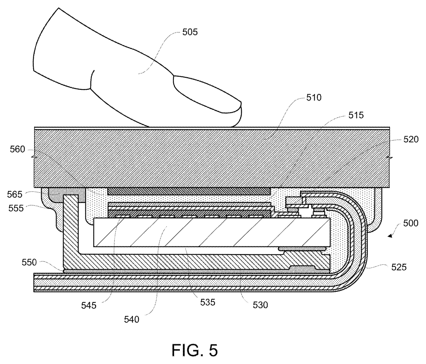
Return to this episode’s first figure. Below the platen (510) the finger presses is the sensor system (500), and what bonds the two is the adhesive (560). It is a layer drawn in the figure and the sound must pass through it. In large-area configurations this place gets thicker still. The same patent places a multi-functional film between sensor and display, and the specification states that the film includes a light blocking layer, an electromagnetic shielding layer, an adhesive layer and a stress buffer layer, with one or more of them in the acoustic path. The adhesive layer is a pressure-sensitive adhesive (PSA) or epoxy, and the spacer is PET. The materials just listed in the table are sitting under the glass exactly as they are.
So how much does this one layer take away? Use the transmission line calculation from Section 3 as it stands, but this time with hard material on both sides of the layer. At 10MHz the one-way transmission comes out like this.
| Adhesive thickness | Z 1.56 (polyurethane) | Z 2.61 (PVB) | Z 3.27 (acrylic) | Z 5.0 (doped epoxy, assumed) |
|---|---|---|---|---|
| 2µm | 88.8% | 98.3% | 99.2% | 99.7% |
| 5µm | 56.2% | 90.2% | 95.4% | 97.9% |
| 10µm | 25.1% | 70.0% | 83.9% | 92.3% |
| 20µm | 9.1% | 38.5% | 57.9% | 76.3% |
| 37.5µm (quarter wave) | 5.2% | 18.7% | 31.9% | 53.3% |
This table is this episode’s title. The cover glass loses essentially nothing over 700 micrometres of thickness. The impedance is continuous so there is no boundary at all, and the attenuation is too small to be worth listing in an acoustic properties table. In the same table every polymer has its attenuation column filled. And yet the adhesive layer under the glass, at 20 micrometres, 1/35 of the glass thickness, can drop one-way transmission to 9%. The place the sound is blocked is not the thick glass but the thin adhesive.
Industry has only two methods, because there is no material whose impedance matches glass.
First, make it so thin it might as well not be there. The 10MHz wavelength in a polyurethane adhesive is 150 micrometres, and taking the thickness down to 1/50 of that, 3 micrometres, brings transmission up to 78%. When a layer is thin enough relative to the wavelength, the sound barely sees it.
Second, raise the material’s impedance. The method from Section 3. Dope the epoxy with particles to change its density. The last column of the table above is that result, splitting 9% from 76% at the same 20 micrometres. The specification the patent attaches to this layer points that way: thickness 15-25 micrometres, speed 1,500-4,000m/s, attenuation 25dB/cm or less (US10891458B2). That the speed’s upper limit is open to 4,000 is the key. An ordinary polymer does not reach that value, and indeed the specification lists one of this layer’s roles as a matching layer between the high-impedance and low-impedance layers. It is where the matching layer attached in front of the piezoelectric layer in Section 3 and the adhesive layer bonding to glass become the same object.
But every table so far is a lossless calculation.
The share of sound absorbed inside the layers was not included. Include it and how far things move in which direction parts glass from polymer once again. Polymer attenuation is broadly proportional to frequency and thickness. Divide the values in the acoustic properties tables by frequency and acrylic comes to about 1.3-2.5, the PET family (PETG) 4.0 and silicone rubber 5.9-8.4 dB/cm/MHz, while glass has that column empty altogether.
Put absorption into the transmission line calculation and run it again and it comes out like this.
| Layer | Lossless | With absorption |
|---|---|---|
| no film (direct contact) | 36.1% | 36.1% |
| tempered glass film 300µm, full contact | 36.1% | 36.1% |
| PET film 63µm (quarter wave), 10MHz | 85.3% | 78.1% |
| PET film 300µm, 10MHz | 68.8% | 49.2% |
| PET film 300µm, 20MHz | 54.3% | 31.3% |
| adhesive layer under glass 20µm | 9.1% | 9.1% |
Three directions are read at once.
First, tempered glass is unchanged with absorption included. That it is acoustically transparent, written above, holds with absorption too. Because it is glass.
Second, PET is shaved as thickness and frequency mount. The 300-micrometre one goes from 69% to 49% at 10MHz and from 54% to 31% at 20MHz. Choosing a film gains one more variable beyond material and thickness: frequency.
Third, the adhesive layer does not move from 9.1% with absorption included. 20 micrometres is not enough distance for absorption to accumulate. Put in the upper limit the patent allows and only the decimals change. The loss in the adhesive layer is mismatch, not absorption, and so there is no route other than changing the material or making it thinner.
The 215 micrometres of silicone rubber on an on-chip sensor sits on the same axis. Its impedance of 1.16 MRayl is the closest of any material to skin, while its attenuation is the largest of the three above. Matching and attenuation run separately. That is why that layer is managed by thickness.
Finally, more layers means more arrival times.
Add one layer and two boundaries appear. The sound travels back and forth inside that layer too, so reverberation returns with a period of 2d/c. Section 5 said this sensor cuts by time, so it seems what arrives late can simply be cut away. Put numbers in and it does not work out that way.
| Layer | Round-trip time in the layer |
|---|---|
| adhesive 20µm | 27ns |
| adhesive 50µm | 67ns |
| PET film 63µm | 50ns |
| PET film 300µm | 236ns |
| cover glass 700µm | 233ns |
The first acquisition time window in the patent quoted in Section 5 is 5 to 50 nanoseconds. The adhesive layer’s reverberation, at 27 nanoseconds, falls inside that window. It is too thin to separate in time, and narrowing the window cuts the real signal along with it.
The other end is awkward too. The reverberation of a 300-micrometre PET film is 236 nanoseconds and the cover glass round trip is 233 nanoseconds. That number from the title of Section 1. The fake arrives at the same time as the real. That is at that thickness, of course, and changing the thickness moves the arrival time. The point is that the time window is not a cure-all. Cutting by time can discard what arrives late; it cannot discard what happens to arrive at the right time.
Hold the thickness at 20 micrometres and push only the impedance slider to the right and what the doping buys becomes visible. Conversely leave the impedance and take the thickness down to 3 micrometres and it reaches the same place. It is why industry uses both methods.
So a decision to add one more layer in this sensor does not end with an impedance calculation. When the reverberation that layer will make arrives has to be looked at too. The impedance that made the contrast in Section 4 and the time window that filtered the noise in Section 5 mesh in the same layer.
8. What the same sensor also does
The end of Section 5 said the time window only needs its values changed. That property becomes a feature.
Spoof detection. A forgery imitating ridges and valleys in silicone or latex may pass the surface pattern but has nothing under the skin. Qualcomm’s spoof detection patent defines the reflected energy signal ratio (RESR), the energy returned from internal structure of an object divided by the energy returned from the whole object, and judges by whether it falls inside the template range of a real finger (US10444335B2). It is the signal caught in the simulator when the window was pushed near 750 nanoseconds.
Force measurement. The multi-functional patent reads pressing force without a pressure sensor. The method is the change in the ridges’ contact area. Press harder and the ridges flatten and spread, increasing the area touching the glass and changing the reflected amplitude of the ridge regions with it (US10438040B2). The physics of contact that obstructed recognition in Section 7 becomes an input signal here. The same phenomenon is both problem and feature.
Harmonic detection. Integer multiples of the transmitted frequency are looked at separately (US10410034B2). They arise when the medium responds non-linearly, so they are used to read tissue properties separately.
Combination with bioimpedance. A configuration measuring the hand’s moisture and oil levels electrically alongside, to correct the matching algorithm, is also in the patents. It is the approach of supplementing with information what physics cannot solve about the dry hand problem of Section 7.
9. Qualcomm’s position, and the companies that entered it
The landscape of this technology belonged to one company for a long time.
In a Google Patents search for titles containing both ultrasonic and fingerprint, US grants number 96, of which 34 are Qualcomm’s (retrieved 28 August 2026). The rest run BOE 10, InvenSense 10, Fingerprint Cards 5, Apple 4 and Goodix 4. A field where one company holds a third is not common.
Look inside those 34 and it is visibly not a scattered bundle of patents. The same names recur on the inventor lists of the multi-functional, time window, harmonic and spoof detection patents cited in this article. It means the output of one team over more than 10 years, which is why the five stages followed in this article mesh together.
The product numbers say the same. 3D Sonic Gen 2 has a sensing area of 64 square millimetres in a package 150 micrometres thick, and 3D Sonic Max reads two fingers at once over 20 by 30 millimetres, that is 600 square millimetres.
Widen the jurisdiction beyond the United States, though, and the picture changes.
On the same title condition, Chinese publications number 378, of which Goodix has 56, Shanghai Silead 25 and BOE 23. Qualcomm has 19. In a title search across all jurisdictions, Goodix’s 73 leads Qualcomm’s 37. The two numbers are not a contradiction; they look at different points in time. Granted patents are the result of the past 10 years, published applications the development now under way.
Lay Goodix’s Chinese publications out by year and the entry point is visible.
| Publication year | 2016 | 2018 | 2020 | 2022 | 2024 | 2025 |
|---|---|---|---|---|---|---|
| Count | 0 | 0 | 4 | 18 | 11 | 20 |
Zero until 2019, starting in 2020, jumping once in 2022 and again in 2025. The company’s own official history records the same points: ultrasonic fingerprint sensor unveiled in 2024, mass commercialization in 2025. The company that put out an optical under-display fingerprint sensor in 2017 and took the market took 7 years to cross to ultrasonic.
The first commercial product is confirmed too. In a press release of 13 May 2024, Goodix stated that its ultrasonic fingerprint solution was mounted at large scale for the first time in the vivo X100 Ultra. What the company led with was not a performance figure but process: handling the acoustic layer at wafer level to simplify the supply chain. The disclosed specification is a sensing area of 5 by 5 millimetres in a module 0.17 millimetres thick.
There is a separate sentence in that press release worth noting, a remark by the company’s president.
“The surging demand for ultrasonic fingerprint sensors in mobile authentication is driven by the rapid evolution of the latest pol-less display technology”
A sensor company explains demand for its own product by a change in display structure. The configuration this series has kept covering repeats here. Change the panel and the sensor beneath it changes. Move to a structure removing the polarizer and putting colour filter and black matrix on the encapsulation, and the optical properties of the screen change, and an optical fingerprint sensor using the screen as illumination takes that change head on. A method that does not use light becomes relatively favoured.
It is the same axis as the polarizer removal enlarging the ambient light sensor’s viewing angle problem in episode 3, and the polarizer being nearly transparent to near-infrared and therefore not the culprit for Face ID in episode 4. The same process change acts in a different direction for each sensor.
One thing needs stating clearly. What is written here is only patent counts and sentences the companies disclosed themselves. Market share and shipment figures are not used. Such figures found by search are mostly summary lines from paid market research reports and there is no way to verify them.
10. What set the axis was not distance but wavelength
The place to close Part 1.
Why under the screen is uniquely hard
Before that, one number has to be settled. The five stages seen so far happen in exactly the same way in a sensor attached directly beneath the finger. Indeed the on-chip PMUT fingerprint sensors the review introduces put only a thin protective layer between finger and transducer. The examples the review gives are silicone rubber (PDMS) at 215 micrometres and aluminium oxide at 1 micrometre.
Under-display puts glass of 700 micrometres or more in that place. Three times the thickness, but thickness is not the only problem. The medium changes the wavelength.
Wavelength is the speed of sound divided by frequency. Silicone rubber’s speed is 1,027m/s and glass’s is 6,000m/s. At the same frequency the wavelength in glass is six times longer. The scale over which a wave spreads while crossing a distance L is roughly the square root of the product of wavelength and distance.
| Condition | Wavelength | Spread | Against a 500µm ridge period |
|---|---|---|---|
| on-chip (silicone rubber 215µm), 10MHz | 103µm | 149µm | 30% |
| under-display (glass 700µm), 10MHz | 600µm | 648µm | 130% |
| on-chip, 20MHz | 51µm | 105µm | 21% |
| under-display, 20MHz | 300µm | 458µm | 92% |
Glass is not a good material for transmitting sound well. It is fast, so the wavelength is long, and the long wavelength smears the pattern. This is why an ultrasonic fingerprint sensor placed directly beneath the finger passed practical resolution long ago while under the screen remains hard.
The numbers industry has produced point exactly in this table’s direction. Qualcomm’s dual-frequency patent gives the first frequency as 10 to 20MHz and the second as 1 to 10MHz, a division of roles: high frequency for the surface, low for under the skin. The 2024 study in Measurement obtained a lateral resolution of 112.48 micrometres with a device of 33MHz centre frequency, less than half a ridge width. Thickness is the same story. That 3D Sonic Gen 2’s package at 150 micrometres and Goodix’s module at 0.17 millimetres lead the specification sheet is not only about space. The thinner it is, the better it sees.
And here the film’s second price appears. A 300-micrometre tempered glass film, acoustically transparent as seen in Section 7, still stretches the propagation distance from 0.7 to 1.0 millimetres. At 10MHz the spread grows from 648 to 775 micrometres. Even with perfect contact the image is a little more blurred. It is loss of the kind where the pattern fades rather than the signal disappearing.
Closing the table of Part 1
Episode 4 aligned the under-screen sensors on a single indicator: the Fresnel number. It is the aperture size squared divided by wavelength and distance, and that one value decides how a wave propagates. Large, and the wave is simply blocked or passed; small, and it spreads by diffraction.
In that table the fingerprint sensor sat at the far right of the axis. With the finger touching the glass the distance is effectively nothing, so the Fresnel number is very large, and the problem was not optical but geometric.
Now read the same finger with sound. Distance and glass are unchanged. Take a ridge half-period of 250 micrometres as the aperture and compute at a stack thickness of 0.7 millimetres and it comes out like this.
| Reading method | Wavelength | Fresnel number | Propagation regime |
|---|---|---|---|
| optical fingerprint (550nm) | 0.55µm | 162 | geometric optics |
| ultrasonic fingerprint (10MHz) | 600µm | 0.15 | diffraction |
| ultrasonic fingerprint (20MHz) | 300µm | 0.30 | diffraction |
| ultrasonic fingerprint (33MHz) | 182µm | 0.49 | diffraction |
Not three orders of magnitude but the opposite end of the axis. Same distance, same glass, same fingerprint, and the optical type is in the geometric optics regime while the ultrasonic type is in the diffraction regime. What separated them is wavelength alone.
With that, the table of Part 1 is complete.
| Sensor | Subject distance | Fresnel number | Propagation regime | Problem faced | Character of the solution |
|---|---|---|---|---|---|
| fingerprint, optical (ep. 5) | contact | very large | geometric optics | light mixing between pixels | cut angle with apertures |
| ambient light (ep. 3) | a few cm and up | about 10 | geometric optics | reduced viewing angle | transmitting window and correction |
| proximity (ep. 2) | mm to cm | about 1 | Fresnel diffraction | background noise | modulation and synchronization |
| camera (ep. 1) | infinity | 0 | Fraunhofer diffraction | blur and flare | restoration and metasurfaces |
| Face ID (ep. 4) | 25 to 50cm | near 0 | diffraction plus correspondence collapse | false depth | reduce the dots |
| fingerprint, ultrasonic (ep. 6) | contact | 0.15-0.5 | diffraction | spread and contact | cut angle with time |
The same thing sits at both ends of the axis: a finger in contact. So the conclusion of Part 1 comes out like this.
What decided this axis was neither what the sensor looks at nor how far away it is. It was wavelength.
Distance looked like the thing making the axis because all five subjects from episode 1 to episode 5 used light. With wavelength fixed and only distance varying, distance looked like the cause. Only after changing the wavelength a thousandfold does what the real variable was become clear.
This conclusion has a practical implication. The first question in designing an under-screen sensor is not where to put the sensor but how many wavelengths across the pattern to be read is. Fix that ratio and the problem to be faced is fixed, and once the problem is fixed so is the character of the solution. On the geometric optics side it becomes a problem of designing what to block; on the diffraction side, a problem of how to undo what has spread.
And the five stages followed in this episode show which layer of the hardware that answer is inscribed in. Material (Section 2), electrode arrangement (Section 3), time window (Section 5), pixel circuit (Section 6). All four sit on conditions the display process set first.
11. Questions left
How far can the frequency be raised? A 33MHz device came out of a laboratory, but production specifications are still in the 10 to 20MHz range. Raising the frequency reduces the spread but increases attenuation and the devices have to get smaller. Where the balance falls sets the next generation’s performance.
What happens in a foldable? A folding screen has ultra-thin glass and several polymer layers instead of glass. More layers means more boundaries, each with a different impedance and thickness. It is a situation calling for the Section 7 calculation applied several times over, and related applications are already published.
How far has impedance imaging come? The second method seen in Section 4. Reading the decay of the ringing instead of the amplitude changes both the role of the time window and the circuit. Which of the two commercial products use is not confirmed in public material.
Is the large-area wall physics or process? The segment seam distortion and the lamination cracking of large-area glass seen in Section 3 are problems of different character. The first can be reduced by design; the second is a yield problem. What sets the date when the whole screen becomes a fingerprint sensor is probably the latter.
Part 1 closes here. Part 2 moves from sensing to emission. It will cover why half the light an OLED makes never gets out of the panel.