HDS, the driving technology that took LG Display OLED TV panels to 165Hz
The best display panel award at IMID 2026 went not to FLiPP but to HDS. Data transmission speed was doubled, yet the refresh rate rose only 15%, from 144Hz to 165Hz. Spend the whole doubling and 288Hz should come out. We followed where the rest went, through the time given to a single gate line.
In the August monthly news LG Display put out on 31 August, two technologies ran side by side. One is FLiPP, a deposition process that does without a fine metal mask, and the other is a driving technology called HDS (Hyper Double Scanning).
Almost every page that week put FLiPP in the headline. But the one that took the best display panel category of the Display of the Year award at IMID 2026 was HDS. Precisely, “Real UHD 165Hz OLED applying HDS technology.” In the same category Samsung Display was selected alongside it with the OLED for the Galaxy S26 Ultra.
The definition of HDS the company gave is one sentence: a technology that doubles data transmission speed compared with the existing one while achieving stable panel driving and a thin bezel through heat-improvement design, control algorithms and in-panel driver circuit design. And the result that appeared in the press is that it raised the refresh rate of an OLED TV panel from 144Hz to 165Hz, about 15%.
Put those two numbers side by side and they do not match. Transmission speed doubled, and the refresh rate rose 15%.
165Hz is only 15% faster than 144Hz
Start by counting how much data this panel actually handles. LG Display’s fourth-generation OLED TV panel is 3,840 × 2,160 resolution at 10-bit colour depth. One pixel is three RGB values and each value is 10 bits, so one frame is 3,840 × 2,160 × 3 × 10 bits.
Multiply by refresh rate and the pixel data rate per second comes out. This is pure pixel data with the vertical blanking interval excluded.
| Refresh rate | Pixel data rate |
|---|---|
| 120Hz | 29.86 Gbps |
| 144Hz | 35.83 Gbps |
| 165Hz | 41.06 Gbps |
| 240Hz | 59.72 Gbps |
| 288Hz | 71.66 Gbps |
What going from 144Hz to 165Hz requires is 14.6% more data. If a transmission speed genuinely twice as fast had been secured and all of it spent on refresh rate, 288Hz should have come out. What actually came out is 165Hz. Of that doubling, the share that went to refresh rate is only 15%, and the rest went elsewhere.
So the question has to change. Why did raising it 15% take a doubling.
The problem is not bandwidth but the time given to one line
A panel does not light the whole screen at once. It opens the gate lines one at a time, puts data into the pixels on that line, and moves to the next. For a 4K panel that is 2,160 lines. One frame time divided by the number of lines is the time given to one line, and this is what governs the actual design.
| Condition | Time given to one line |
|---|---|
| 144Hz, whole screen at once | 3.215 µs |
| 165Hz, whole screen at once | 2.806 µs |
Going up to 165Hz makes the time given to one line 12.7% shorter. This is where the trouble starts.
The circuit that opens the gate lines is, in large panels these days, built directly onto the glass rather than being a separate chip. Gate driver in panel, GIP as the industry calls it, and cases applied to 55-inch and 65-inch UHD OLED have been reported at conferences. This circuit runs in a long vertical strip along the outer edge of the screen. The width that circuit occupies is the bezel.
As the time gets shorter the circuit has to get stronger. A gate line is long and has pixels hanging off it in a row, so its resistance and capacitance are large. Charging that load in a short time means making the transistors bigger, and bigger transistors make the circuit wider, and by that much the bezel gets thicker.
Yet what LG Display announced is the opposite. It said the bezel got thinner while the refresh rate rose. That is not a combination that can come out of simply raising the refresh rate.
Split the screen in two and the numbers turn over
There is only one way to lengthen the time given to one line. Reduce the number of lines one circuit is responsible for. Divide the screen into upper and lower regions and scan them at the same time, and each region takes only 1,080 lines.
| Condition | Time given to one line | vs 144Hz |
|---|---|---|
| 144Hz, one region | 3.215 µs | baseline |
| 165Hz, one region | 2.806 µs | −12.7% |
| 165Hz, two regions at once | 5.612 µs | +74.5% |
The numbers turn over. Split into two regions and even at 165Hz one line is given 5.612µs. That is 74.5% more comfortable than at the previous 144Hz. The refresh rate went up and yet the gate circuit got easier. By as much as it got easier the transistors can be made smaller, and so the bezel gets thinner.
The technology being named Double Scanning also fits this reading. And it is not a newly invented concept. That 8K panels need dual scan on both the source and gate sides is already an industry premise, and a structure driving a dual-scan OLED panel split top and bottom appears in the literature. Dividing gate driving into regions to reduce RC delay in large panels is also being studied on the automotive OLED side.
The source driver pays the price
It is not free. Drawing two regions at the same time means data has to be pushed into both regions in the same instant. The load on the source side that supplies the data doubles exactly.
This is what the sentence “doubled the data transmission speed” points to. Not a doubling to make the refresh rate double, but a doubling to feed two halves of the screen at once.
On top of that comes the 14.6% refresh rate increase. Driving two regions at once at 165Hz makes the source-side pixel data rate 82.1 Gbps, 2.29 times the previous 144Hz single-region driving.
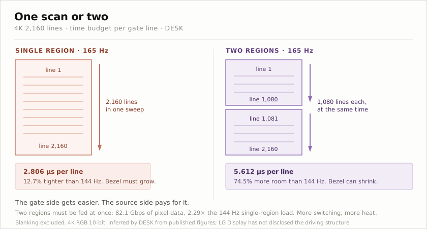
And that price comes back directly as heat. That dividing the screen into several driving regions raises source driver power consumption, because the number of charge and discharge cycles goes up, is known. This is why the announcement went out of its way to include “heat-improvement design and control algorithms.” Not one more thing to boast about, but better read as saying it also solved the problems this structure creates.
But speed is not the only thing the source side pays. The wiring structure changes.
Data lines run vertically across the whole screen. Open a row in the upper half and a row in the lower half at the same time and two pixels hang on the same data line, so different values cannot be put into them. For split driving to work, the data line has to be cut in the middle so that top and bottom each have their own source driver.
There are two ways. One is to put source drivers on both the top and the bottom. A structure dividing the screen into two regions with a master chip driving one side and a slave chip the other is set out in a patent, and on 8K panels dual scan is a premise on the source side as well as the gate side.
This way, though, doubles the driver ICs and COFs and raises cost. It is hard to put forward a configuration that raises cost as a new technology.
The second way is more plausible. Keep the source IC on one side and have one channel feed several lines in turn. Put a multiplexer inside the panel to split one channel’s output across several wires, and the IC count and the channel count stay the same while only the wiring increases. In exchange one channel has to send several shares in the same time, so the transmission speed per channel rises by that much.
The wiring that takes the lower half passes through the upper half on the way down but does not touch the pixels in that stretch. It is not cut but merely passing through, running as a single line from the multiplexer to the bottom edge of the screen.
How many ways the multiplexer was set is unknown. Two is the simplest, but configurations of four or more that also reduce the channel count are common. Either way the principle is the same. Instead of adding channels, the channels are run faster.
Read the announcement again and it fits this configuration. The sentence double the data transmission speed compared with the existing one does not mean the total data on the panel doubled. The total put onto the screen is set by refresh rate and rose only 15%. What doubled is the speed one channel carries. And since a multiplexer is a circuit built onto the panel glass, the phrase in-panel driver circuit design attached to the same sentence points precisely to that place.
Then the bezel is explained too. Gate drivers sit on the left and right of the screen and source COFs attach top and bottom. Keep the source on one side and top and bottom stay as they are, while split driving reduces the gate load so the left and right bezels get thinner. Had it been the way with drivers on both sides, top and bottom would have grown and it would have been hard to say the bezel got thinner.
This is, though, an inference worked back from the announcement and the cost structure. The company did not say it used a multiplexer, nor that it kept the source on one side.
The reason for putting in a multiplexer is expected to be cost reduction. It allows only the wiring to be increased without adding source ICs and without changing the channel count. Compared with the way of putting drivers on both top and bottom, the ICs and COFs come to half. This too, though, is not something the company stated but an expectation worked back from the cost structure.
Split the screen and a line appears down the middle
Split driving has one more side effect that is hard to avoid. The boundary.
Because top and bottom are driven by different circuits, small differences gather at the middle of the screen. If gate driving timing slips a little or charging conditions differ, that difference shows at the boundary as a horizontal band of different brightness or colour. The industry calls it stitch. Unlike deviation spread evenly over the whole screen, it concentrates in one line and so is far more visible.
This problem is expected to have been solved. If it came out as a production panel and won an award, it would not have been shipped with the boundary visible. The control algorithm the announcement listed alongside “heat-improvement design” appears to point to that place. Measuring the difference in upper and lower driving conditions and finely correcting the data of pixels near the boundary is the usual approach.
The company did not mention stitch, though. Neither how it was handled nor how far. The above is an expectation drawn from the fact that split driving always meets this problem and that the product actually shipped.
Summarised, HDS is this trade.
| Direction | |
|---|---|
| Source (data) side | tightens 2.29 fold → power, heat |
| Gate side | loosens 1.75 fold → thin bezel |
| Result | 165Hz, and a narrower border |
This far is disclosed, and from here it is inference
One thing has to be made clear. LG Display has not disclosed the driving structure of HDS. What the announcement holds is results only. Double the transmission speed, 165Hz, a thin bezel, improved heat.
Taking the screen as split into two regions above is because the disclosed figures point that way. Raising the refresh rate while shrinking the bezel requires lengthening the time given to one line, and that leaves no choice but to reduce the number of lines one circuit handles. The name fits it too. But this is working back, not confirmation.
Exactly how many regions it was divided into, whether the dividing boundary is the middle of the screen or not, whether gate drivers were put on both left and right or on one side only, how the data lines were divided, whether a multiplexer was used, and how the stitch at the boundary was handled are all unknown. Nor was it disclosed how many millimetres the bezel actually came down to from what. If those values come out, the calculation above has to be matched against them again.
Outlook
Split driving like HDS will become the default for high refresh rate large panels. The reason is in the physics. The resistance and capacitance of a gate line grow as the screen gets larger, and the time given to one line shrinks in inverse proportion to refresh rate. The two curves move in opposite directions, so pushing both size and refresh rate together means they must meet at some point. There is no way to postpone that crossing other than dividing into regions.
Continuing to raise the number of splits, though, will not last long. The finer the division the easier the gate side gets, but the source-side data rate is multiplied by exactly the number of splits. Heat reaches its limit first. The next contest will move from the number of splits to how much less hot the source driver gets at the same data rate.
Whether this forecast was right or wrong can be seen from four things. First, whether LG Display raises the number of splits when it brings out a refresh rate above 165Hz, or uses another method. Second, whether large screens stay at lower refresh rates than small ones in the same generation. Gate lines get longer and the load bigger as the screen grows, so if the limit shows up first in large sizes, it matches this article’s explanation. If the same refresh rate is laid down regardless of size, another trick was used. Third, whether a competitor brings out the same structure under another name. Fourth, whether the company states the bezel width as a number.
The fourth is the most honest indicator. There is a claim that it got thinner but not yet how much thinner. When that number comes out, this article’s calculation gets marked along with it.