MicroLED Leaves the Screen for the Space Between Chips
As the bottleneck in AI data centers shifts from compute to wiring, microLEDs developed for displays have been called up as the light source linking chip to chip. Microsoft's MOSAIC, winner of the SIGCOMM 2025 Best Paper award, packs 400 of them into 1mm² to deliver 800Gbps. That number, 400, wasn't picked at random. And on October 1, ₩13.6 billion in Korean capital flowed into that ecosystem.
This Week's Hot Issue
This column gathers the display industry news that broke over the past week (Monday through Sunday) and digs a little deeper into the single hottest issue among them.
News the Press Covered, September 28 to October 4
This week was split roughly half and half between policy and process stories, with one investment slipping quietly through in between.
First, OLED overtook LCD in smartphones for the first time ever. Its share hit 60.5%. As OLED became standard even in mid- and low-priced models, China-led shipments of smartphone LCDs fell from 930 million units to around 500 million, while Samsung Display and LG Display’s combined share rose from 53.8% to 57.3%.
Second, displays were called a national security asset. At a National Assembly policy forum on October 1, Samsung Display and LG Display both said that “going it alone has its limits.” They asked the government to extend the carry-forward period for tax credits and to adopt a direct refund system that pays credits out in cash even in loss-making years. One figure that came up alongside stood out: LG Display said that by bringing AI into panel circuit design, it had cut work that used to take a month down to 8 hours.
Third, Apple’s shift to OLED in IT devices started getting dates. The first foldable iPhone, the Duo, was confirmed for an October 23 launch, with initial volumes in the 6 million to 8 million range. Reports said a MacBook Pro with an OLED touchscreen would be unveiled in October, and a 6-inch smart home display hub will be revealed on October 13.
Fourth, glass substrates blurred the line between displays and semiconductors further. BOE said it would invest in a mass-production line for semiconductor glass substrates within a year, and YMT said it would expand its electroless copper plating capacity for through-glass vias from 300 sheets a month to 1,200–1,500. A patent application also surfaced from a founder with a display background who solved copper plating delamination using the adhesion principle of mussels. We covered glass-core substrates in a full article in Issue 4, so we won’t unpack them again here.
Fifth, in maskless processing, a declaration and a product collided one day apart. On September 28 in Beijing, BOE said non-FMM photopatterning “has not been proven for mass production,” and the very next day a product launched carrying a display made with Visionox’s ViP maskless process. It’s 1.5 inches, 466×466, at 5,500 nits, and was introduced as the first commercial display made without a mask. On September 30, TCL CSOT announced it would take the inkjet route all the way. We covered maskless patterning in depth in Issue 2, so here we only note the events.
Sixth, October utilization was forecast to drop by 3 percentage points. A market research firm attributed it to the three Chinese makers’ National Day production cuts overlapping with Korean panel makers’ conservative inventory management. September exports hit a record $120.9 billion overall, yet displays alone fell 9% year over year.
The hottest issue of September 28 to October 4 is “microLED optical interconnects.”
MicroLED Has Left the Screen
Between September 28 and October 4, three signals pointed to the same place.
On September 29, a wave of high-speed optical interconnect technologies using microLEDs was unveiled at the International Optoelectronics Exposition. On October 1, word came that Korean venture capital firm InterVest had invested $10 million in U.S.-based Avicena. And on October 2, the market reacted to the microLED-dedicated test system Teradyne had launched on September 22, sending its stock up 7.54%.
None of the three stars a display company. Yet all three are microLED stories.
This is a trend of using microLEDs not as screens but as light sources. They’re being used to replace the electrical wires between chips with light. The very device the display industry has spent more than 10 years asking “when will it get into TVs?” has opened first at an entirely different door.
Copper Can’t Go Past 2 Meters, and Optics Fails 100 Times More Often
The backbone of this trend is the MOSAIC paper, for which Microsoft researchers won the Best Paper award at ACM SIGCOMM last year. The paper’s starting point is the wiring problem in AI clusters.
| Copper | Optics (laser) | |
|---|---|---|
| Reach | Under 2m | Tens of meters |
| Power | Efficient | Far more |
| Failure rate | Low | Up to 100 times copper’s |
The paper likened this to the CPU memory wall and called it the networking wall. Use copper and everything has to fit inside a single rack; stretch it with optics and power and failures follow.
Attach numbers and it gets clearer. The paper wrote that had NVIDIA connected 72 GPUs with optics, it would have cost an extra 20kW per rack — the equivalent of 20 GPUs. So it crammed everything into one rack, and that rack came to draw 120kW, requiring complex liquid cooling. Apply the typical failure rate of an 800Gbps link and a link drops once every 6 to 12 hours. AI jobs are synchronous, so when one strand breaks, everything stops.
Trading Few-and-Fast for Many-and-Slow
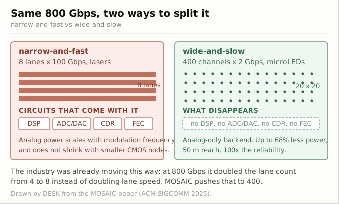
MOSAIC’s idea fits in one sentence. Don’t run channels narrow and fast — run them wide and slow.
A conventional 800Gbps link is eight 100Gbps channels. MOSAIC builds the same 800Gbps out of 400 channels at 2Gbps each. It’s a 20×20 array, and it takes up less than 1mm².
The crux is what changes when you slow each channel down. High-speed optical links come with digital signal processing, analog-to-digital conversion, and clock recovery circuits. What actually eats the power isn’t the light — it’s these circuits. Slow the channel down and those circuits become unnecessary altogether. Only an analog back end remains.
Here are the resulting figures the paper presented. Power is cut by up to 68% compared with conventional optical links, reach is 50m, more than 10 times copper’s, and reliability is 100 times that of conventional optical links. The prototype ran on 100 channels × 2Gbps.
Viewed per cable, the savings come to more than 10W apiece. Microsoft estimated that, scaled worldwide, this adds up to about 100MW a year.
The Industry Was Already Halfway There
This idea didn’t come out of nowhere. The evidence the paper cites is interesting.
Up through the 400Gbps generation, the optical communications industry advanced by doubling channel speed every generation. But in the 800Gbps generation it couldn’t. When 200Gbps per channel proved difficult, it chose to double the channel count, going from 4×100Gbps to 8×100Gbps.
It had already given up on speed and gone for width. MOSAIC essentially pushed that direction to its end — not to 8, but all the way to 400.
The Reason Power Won’t Come Down Lies in Analog, Not Digital
There’s also an answer to why raising speed is so hard. The power of analog components such as drivers, clock and data recovery circuits, and analog-to-digital converters grows in proportion to modulation frequency, and unlike digital logic, it barely shrinks as you move to finer process nodes.
As speed rises, optical margins shrink too. Aging, laser wavelength drift with temperature changes, mechanical stress, and the effects of dust and humidity all grow larger. And the cost per channel is too high to add redundancy. Fast channels are expensive; because they’re expensive you can’t keep spares; and because there are no spares, one failure breaks the link.
Slow channels cut that chain clean through. They’re cheap, so you can lay down many; there are many, so you can survive a few dying.
Why 400, of All Numbers
One question remains here. Where did the number 400 come from? If you’re going to run slow, 1,000 would work, and so would 100.
Here is the order the paper gives. Assuming 2Gbps per channel, an 800Gbps link can be built from a 20×20 array, and that fits inside 1mm². In other words, 2Gbps is set first, and 400 follows from it.
So the question moves one step back: why 2Gbps, of all speeds? The paper doesn’t separately explain why it chose that number. From here on, this is a reconstruction from published figures — this article’s interpretation, not the paper’s argument.
The clue lies in the speed the device can deliver. The modulation bandwidth France’s CEA-Leti reported for a 10µm blue microLED is 1.8GHz. The result showed that smaller emitting areas raise bandwidth, and it ranks among the highest known to date.
One caveat has to be attached here. CEA-Leti achieved 7.7Gbps with that device, but that figure was obtained by layering on multicarrier modulation and digital signal processing. And digital signal processing is precisely what MOSAIC sets out to eliminate. Reattach the DSP and the power advantage vanishes. So within MOSAIC’s arithmetic, we have to assume the simplest modulation, and at that point the speed 1.8GHz can deliver is just over 2Gbps.
Divide 800Gbps into N channels and each channel runs at 800÷N, and the device has to be fast enough to deliver that speed.
Step the slider down one notch at a time and the boundary reveals itself.
| Array | Per channel | Bandwidth the device must deliver | |
|---|---|---|---|
| 6×6 = 36 | 22Gbps | 19GHz | Laser and DSP territory |
| 13×13 = 169 | 4.7Gbps | 3.9GHz | Still far off |
| 19×19 = 361 | 2.2Gbps | 1.85GHz | Just barely over 1.8GHz |
| 20×20 = 400 | 2.0Gbps | 1.67GHz | First becomes possible here |
19×19 falls short; 20×20 is where it first gets there. And 20×20 is exactly the number MOSAIC used.
It could be a coincidence. But take the two published figures (1.8GHz and 800Gbps), run a single conversion assuming the simplest modulation, and the boundary lands at 371 channels; round to a square and 20×20 is the first fit. As one reading of where the 2Gbps value came from, it holds together.
In practice they lay down more than 400. The paper wrote that adding a few spare channels, or laying down generously, greatly raises link reliability while also reducing the complexity and power of the electronics. It said the burden on power and cost is negligible. It’s a choice made possible because slow channels are cheap.
And That Size Is Exactly MicroLED
One more thing falls out of the same calculation. To fit 20×20 into 1mm², the pitch is 50µm. That value is set by geometry, so there’s no room to argue. The pitch puts an upper limit on device size, and taking roughly 1/10 of the pitch gives 5µm. The 1/10 is an assumption this article made, not a value the paper stated.
5µm is the size of a microLED. The very dimension the display industry has been shrinking pixels toward becomes, here, a requirement as is.
So “why microLED?” and “why 400?” were the same question. And there’s a single answer. You have to come down to that size to get that speed, and at that speed you have to lay down that many.
The paper gives two reasons for choosing microLEDs. Their structure is simple and insensitive to temperature, making them more reliable than lasers, and an industry that has already built 500,000 of them in a tiny area exists. High-resolution displays for head-mounted devices and smartwatches have built up that experience.
MicroLEDs Spray Light in Every Direction
Up to this point microLEDs might seem all upside, but the problem the paper worked hardest to solve lies elsewhere: the shape of the light.
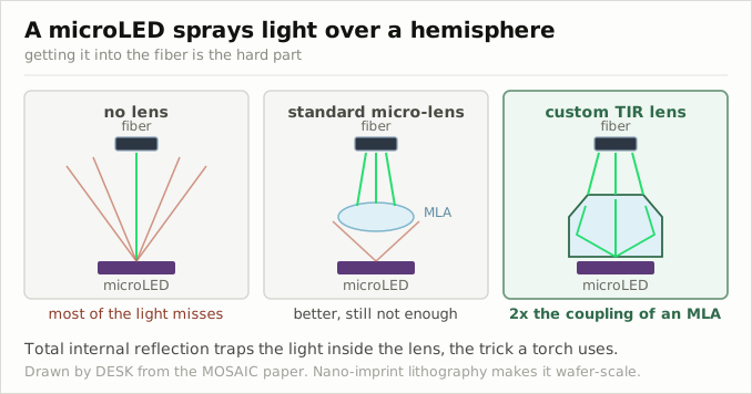
A laser emits a beam gathered in one direction. A microLED is a Lambertian emitter, so its light spreads across the entire hemisphere. As is, it’s hard to get into an optical fiber, and worse, it leaks into neighboring channels. With 400 laid down in 1mm², crosstalk becomes an immediate problem.
The researchers first tried a standard microlens array. Coupling efficiency improved, but it couldn’t capture enough light. So what they designed instead was a lens that uses total internal reflection (TIR). It works on functionally the same principle as the reflector in a flashlight, and it’s a two-part micro-optical structure.
By trapping light inside the lens, it raised coupling efficiency more than 2 times over standard microlenses. And the value of this design isn’t only efficiency. Despite its unusual shape, it can be mass-produced at wafer scale with nanoimprint lithography. Good performance is useless if you can’t stamp it out, and it satisfied that condition at the same time.
Running slow pays off here too. A microLED’s spectrum is broad, at 10nm or more, which makes chromatic dispersion a problem, but at low channel speeds its effect becomes small. So it can be corrected with only a low-speed analog equalization circuit, without digital signal processing.
The Fiber Never Touches the LED
Even once the device is ready, the job of getting light into the fiber remains. This is where packaging is won or lost.
The structure stacks from the bottom up. A lens array sits on top of the microLED array, and a ferrule covers that, holding the optical fiber. The fiber doesn’t touch the LED directly; instead, the TIR lens described above gathers the spreading light and hands it to the ferrule. The receiving side has the same structure. The paper wrote that it placed TIR microlenses on both the microLEDs and the CMOS sensor array. The evaluation kit Avicena unveiled likewise mounts LEDs, photodetectors, and microlens arrays together on top of an ASIC.
The fiber it uses is unusual. It’s not a telecom fiber but an imaging fiber for medical endoscopes. It’s a mass-produced product, and a single strand holds up to 10,000 cores.
The choice the paper made here matters. It uses a single strand, not a bundle of many individual fibers. Because it’s drawn in one process, every core has nearly the same loss and chromatic dispersion, and nearly the same length. So skew between channels is negligible. The paper calculated that even a 1cm length mismatch produces only a 50ps delay difference — 10% of a 2Gbps bit period, which is easily tolerated.
It’s Not One LED per Core
This is the most counterintuitive part.
With 10,000 cores and 400 channels, you could match them 1:1. The paper itself wrote that this is “possible in principle.” But it didn’t do that.
Since there are cores to spare, it sends the light from one microLED across several cores. There’s one reason: it greatly relaxes the alignment accuracy required.
The weight of this choice is clearer to those who know mass production. If 400 channels had to be matched one by one to 400 cores, that alignment process would be the yield and the cost. Spill one into many and that problem disappears entirely. The alignment-and-yield fight displays have waged in mass transfer, this design sidesteps from the start.
Korean Money Went In, but No Korean Company’s Name Appears
Back to the October 1 investment.
The $10 million InterVest put into Avicena is ₩13.63 billion, and with it InterVest took a 1.77% stake. Avicena’s cumulative funding is $130 million, and SK hynix participated in its earlier $65 million Series B.
But SK hynix’s own technology is on a different path. In a paper published in Nature Electronics this past August, what SK hynix proposed was silicon-photonics-based CPO and an optical interposer — not microLEDs. The target figures it cited are bandwidth above 100Tbps, under 1pJ per bit, and chip-to-chip latency under 10ns. As it happens, the energy-per-bit target sits at the same mark as the value Avicena has put forward. That means the two paths are aiming at the same point; where they part is in what makes the light.
In other words, the same company has bets on both paths. While its own technology heads toward silicon photonics, it has staked out a position on the microLED side through investment. It’s a setup that keeps it from losing outright whichever side wins.
The problem is that no Korean company’s name appears on that ecosystem map. The microLED optical interconnect ecosystem compiled by a market research firm lists Microsoft and Marvell on the system side; Avicena, ams OSRAM, and Taiwanese and Chinese firms for light sources; TSMC for photodetectors; AUO, PlayNitride, and Innolux for system integration; Credo for cables; and Aledia and CEA-Leti in Europe. Korea is in only through capital.
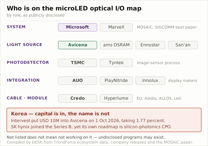
Still, “not visible on the published map” and “not participating” are different things. In Korea, too, there are companies that have said they will extend microLED backplane technology into optical communications for AI data centers. There may be undisclosed development, and this article was unable to confirm whether there is.
The Gate Is Inspection, Not the Device
Iris 100, which Teradyne launched on September 22 at the European Conference on Optical Communication, drew a response in its share price on October 2. It’s an optical test system dedicated to microLEDs.
What it does is simple. It measures every individual emitter in the array, one by one. It measures spectrum, per-pixel luminance, and uniformity, and catches dead pixels and clustered defects early in the process. It targets two markets: microdisplays for AR and optical I/O for AI data centers.
Why inspection is the gate becomes clear in numbers. A single 400-channel link has 400 emitters. If even one dies, that channel goes empty. Avicena splitting the 320 channels in its evaluation kit into 256 active and 64 spare follows the same logic. Instead of preventing defects, it absorbs them by design.
The display industry already has the technology to make the devices. The final lock on commercialization is the equipment to measure and screen them by the millions. The significance of this announcement is that semiconductor-grade inspection has entered microLED.
What Remains
Here is what has not been confirmed.
Mass production timing is still at the preview stage. The evaluation kit came out in March 2026, and there’s no industry standard. In its blog, Microsoft said only that it is working with suppliers to productize and scale up to mass production, without giving a date. The absence of a standard also means the years from 2026 on will be a period of fighting for control of the specification.
The energy figures are based on manufacturer announcements. At a drive current of 100µA per LED, Avicena put forward 80fJ/bit for the transmitter, and under 1pJ per bit for the full link. It also offered a comparison with competing optical approaches at around 5pJ/bit. But these are evaluation-kit and demonstration figures, not values reproduced under mass production conditions.
Market size forecasts are still small. A market research firm put revenue from microLED-based CPO modules at around $848 million in 2030. Compared with the overall AI optical transceiver market, estimated at $26 billion in 2026, that’s in the single-digit percent range.
And one thing this article couldn’t answer. What Korean panel makers and materials, parts, and equipment suppliers are actually doing in this field could not be confirmed from public sources. We don’t conclude that they’re doing nothing.
Outlook
This trend shows that while the display industry waits on microLED with the question “when will it get into TVs?”, the first high-volume demand for the device may open up outside the screen. News that microLED had been pushed out of wearables and a forecast that shipments will grow 10-fold by 2030 came out at the same time and seemed to contradict each other — but they don’t; the applications are shifting.
Here are three things component makers should be watching now.
First, will mass transfer and inspection technology carry over as assets? Optical I/O demands exactly the work of moving and measuring pixels. But the required volumes and defect criteria differ from displays. How far existing equipment and processes can be used as is will determine how wide the door opens for Korean materials, parts, and equipment suppliers.
Second, will Korean company names appear on the ecosystem map? For now only capital has gone in. The watch point is whether, by the first half of 2027, a Korean panel maker or materials and equipment supplier announces a supply contract or joint development in this field. Without such an announcement, once again the technology will be completed abroad and we’ll be on the buying side.
Third, will the 1.8GHz ceiling rise? The number 400 today is a value set jointly by that ceiling and the condition of “no DSP.” If devices pass 3GHz, the same 800Gbps can be built with half the channels, and packaging and fiber requirements change wholesale. Watching whether this number moves tells you how far this technology will go. Conversely, if the ceiling stays put, scaling will happen only by adding channels, and display-style high-volume manufacturing capability will matter all the more.