Splitting the job across a double seed layer: transparency and electron injection in a transparent QLED electrode
To build a screen that becomes a window when it goes dark, the electrode laid on top has to pass light, carry current and push electrons in as well. Lay silver down at 10 nanometres and it works, except that silver at that thickness grows scattered like islands. A team at Pusan National University and DGIST laid the seed layer in two layers rather than one and split the roles between them.
DOI 10.1002/nap2.70283A display that becomes a window when it switches off is an old picture. A shop window turns into an advertising board, instruments appear on car glass, a building window becomes a sign. Quantum dot light-emitting diodes (QLED) suit that picture well: colour purity is high, they can be solution processed, and colour can be set by size.
Yet the last gate to making a device transparent is the single electrode layer laid on top. The lower electrode can be ITO glass, but the upper one has to go on top of organic and quantum dot layers already stacked up. And three things are demanded of that one layer.
Light has to pass through, current has to flow, and electrons have to be pushed into the emitting layer.
The joint work by Pusan National University and DGIST published in Nanophotonics this week starts from the point that those three cannot be held at once by a single material. To put the conclusion first, it laid the seed layer not in one but in two layers and divided the roles, standing all three up together. The result was a transmittance of 63.48% and a sheet resistance of 7.35 Ω/sq at a silver thickness of 10 nanometres, with device efficiency doubled and lifetime tripled.
1. Why the electrode on top is hard
There are many transparent electrode candidates. Yet come to the position of the upper electrode of a transparent QLED and they fall away one by one. Setting out what the paper’s introduction gathers:
- Transparent conducting oxides (ITO, IZO) are laid down by sputtering. High-temperature processing is often needed, and sputtered particles strike and damage the functional layers below. Cost also rises.
- Metal nanowires, carbon nanotubes and conducting polymers can be printed at low temperature. But they use solvent inks in a wet process, which dissolves or swells the layers below or contaminates the interface. The surface is rough and adhesion is weak. PEDOT:PSS corrodes neighbouring layers through its hygroscopicity and acidity, and its conductivity falls over time.
- Graphene needs transfer and lamination, which makes it hard to lay down uniformly over large areas without defects, and its performance leans on chemical doping that is itself unstable over time.
What is left is ultrathin metal laid down by thermal evaporation. Being done in vacuum it does not wet the layers below, it can be spread uniformly over a wide area, and the process is simple. Of the metals, silver is good in both conductivity and transparency across the visible range.
The problem is how silver grows when it is thin.
2. Why silver grows in islands
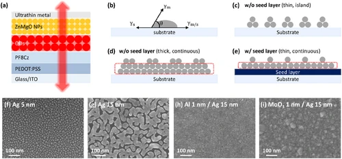
The growth of a metal thin film is set by a balance of three energies: the substrate surface energy, the metal surface energy, and the interface energy between them.
When the force binding metal to metal is stronger than the force binding metal to substrate, the metal does not spread flat but gathers into three-dimensional islands. This is Volmer-Weber growth.
With silver this condition is met far too easily. By the values the paper cites, cohesion between silver atoms is about 1.25 J/m², while the surface energy of the oxide or glass the silver sits on does not reach 0.1 J/m². The gap is more than tenfold, so silver starts as islands from the beginning.
Keep depositing and the islands grow, meet, and finally form a continuous film. So for silver to become electrically continuous it has to pass a certain thickness, and the moment it passes that thickness it begins to block light. This is exactly where transparency and conductivity collide head on.
In practice silver laid down without a seed layer only gave a measurable sheet resistance at 15 nanometres. At 8 and 10 nanometres the film was broken and the resistance could not even be read.
3. What a seed layer does, and the column nobody looked at
The remedy is known. Lay down a very thin seed layer before the silver so that the silver adheres well to the substrate. Lower the interface energy or effectively raise the substrate surface energy, and it leaves the condition for growing as islands. MoO₃, gold and aluminium have been used that way.
The effect was clear. With a seed layer, the film joined up even at 8 nanometres and sheet resistance could be measured.
Here, though, is the blank the paper points to. Seed layer studies so far have mostly filled only two columns, transmittance and sheet resistance. How well that electrode injects charge inside a finished device has hardly been looked at.
In a structure where the upper electrode serves as the cathode this is decisive. If electrons cannot be pushed toward the emitting layer, the device is not bright however transparent it is and however low its resistance. And when the balance of electrons and holes breaks, it is not only efficiency that falls but lifetime that is cut with it.
4. The more uniform one was less transparent
Put the two seed layers side by side and measure, and something comes out against expectation.
| Seed layer | Ag 8nm | Ag 10nm | Ag 15nm |
|---|---|---|---|
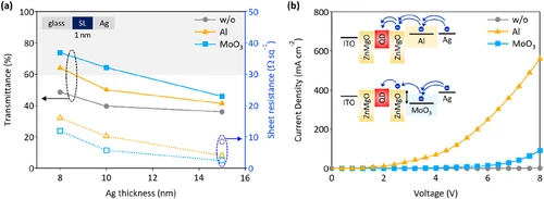
| None | 48.64% / not measurable | 39.62% / not measurable | 36.01% / 8.52 |
| Al | 64.16% / 16.08 | 50.07% / 10.23 | 41.35% / 4.03 |
| MoO₃ | 73.91% / 11.92 | 64.31% / 5.68 | 45.96% / 2.44 |
Under the electron microscope the Al seed side is covered more evenly. Yet transmittance is higher on the MoO₃ side. At 10 nanometres it is 50.07% against 64.31%, a difference of 14 points.
The paper’s explanation is this. Transmittance is not set by the morphological continuity of the film alone. The optical loss the seed layer itself creates and the optical boundary conditions at the interface act together. Metallic aluminium has a large extinction coefficient in the visible, so even at less than a nanometre it causes parasitic absorption and raises effective reflectance. MoO₃, by contrast, is a wide bandgap oxide with a small extinction coefficient, and on top of that it changes the optical impedance of the interface and suppresses reflection.
Then what about electron injection. The order reverses.
Measured with electron-only devices, the Al seed side injected far better. The effective work function of the cathode stack, measured by ultraviolet photoelectron spectroscopy, explains why.
| Stack | Effective work function |
|---|---|
| ZnMgO / Ag | 4.70 eV |
| ZnMgO / Al / Ag | 4.43 eV |
| ZnMgO / MoO₃ / Ag | 4.58 eV |
The one with Al is lowest. A lower work function favours pushing electrons in, which agrees in direction with the clearly higher current density on the Al side in the electron-only devices.
Summarised, it splits like this. MoO₃ is transparent and low in resistance but poor at injecting electrons, and Al injects electrons well but is less transparent.
5. So they stacked them
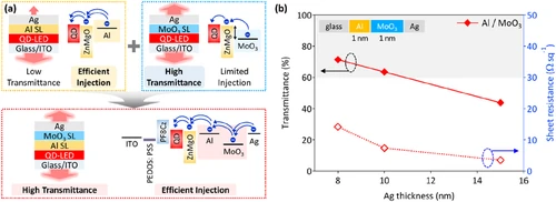
The team’s choice was not to pick one of the two. Lay down 1 nanometre of Al and 1 nanometre of MoO₃ in turn, then 10 nanometres of silver on top.
The roles divide. The lower Al meets the ZnMgO electron transport layer and lowers the electron injection barrier, while the upper MoO₃ lets the silver spread well and takes care of transmittance and sheet resistance.
The result is this.
| Seed layer | Ag 8nm | Ag 10nm | Ag 15nm |
|---|---|---|---|
| Al / MoO₃ | 71.41% / 14.17 | 63.48% / 7.35 | 43.78% / 3.51 |
At 10 nanometres it held 63.48% transmittance, effectively the same level as MoO₃ alone (64.31%). Adding one more Al layer and losing almost no transmittance is the point of this combination.
Why is that. Measuring reflectance gave the answer. The reflectance of the Al/MoO₃/Ag electrode was much lower than Al/Ag and close to MoO₃/Ag. The MoO₃ layer changed the optical boundary conditions of the stack and suppressed interface reflection, offsetting the optical penalty the Al brought in. Steps measured by atomic force microscopy at 11 to 12.5 nanometres matched the design values, confirming the layers stacked as intended.
Sheet resistance is 7.35 Ω/sq, higher than MoO₃ alone (5.68) but lower than Al alone (10.23). None of the three is the best, but all three are put in a usable place, and that was the aim of this design.
6. Twice over in the device
A better electrode and a better device are different things, so actual devices were made and compared.
The structure is ITO / PEDOT:PSS / PF8Cz / red quantum dots (CdZnSe core with ZnSe, ZnSeS and ZnS shells) / ZnMgO nanoparticles / upper transparent electrode.
The basis for choosing what to compare is stated too. To be perceived as transparent, transmittance usually has to pass 50%, and even when the electrode passes that mark the device as a whole comes down further because of reflection, absorption and scattering in the multilayer stack. So a 60% bar was set for the electrode, and MoO₃ alone (64.31%) and Al/MoO₃ double (63.48%), which passed it, were compared. Al alone at 50.07% fell short and was left out of the main comparison.
Summing emission upward and downward gives this.
| Seed layer | Direction | Max luminance (cd/m²) | Max current efficiency (cd/A) | Max EQE |
|---|---|---|---|---|
| MoO₃ | Up | 8,238 | 1.70 | 1.18% |
| MoO₃ | Down | 24,318 | 5.12 | 3.64% |
| MoO₃ | Sum | 32,556 | 6.78 | 4.82% |
| Al/MoO₃ | Up | 20,118 | 4.28 | 2.86% |
| Al/MoO₃ | Down | 51,436 | 10.31 | 6.95% |
| Al/MoO₃ | Sum | 71,554 | 14.59 | 9.81% |
Both luminance and efficiency rose more than twofold. Better electron injection brought the balance of electrons and holes into line.
Lifetime followed. Driven at constant current from an initial luminance of 10,000 cd/m², the time until brightness fell to 70% (T70) was 5.81 hours for MoO₃ alone and 18.56 hours for the Al/MoO₃ double, 3.2 times. The paper explains that poor electron injection creates charge imbalance, which enlarges non-radiative loss paths such as Auger recombination and interface quenching and brings degradation forward.
🔴 The paper also converts these values to a 100 cd/m² basis and writes 73,888 hours and 23,130 hours. Those two numbers are not measured but extrapolated. They come from putting n = 1.8 into the acceleration relation L₀n·T70 = constant, while what was actually measured is 18.56 hours and 5.81 hours at 10,000 cd/m². What can be used for comparison is the multiple (3.2 times), not the absolute values.
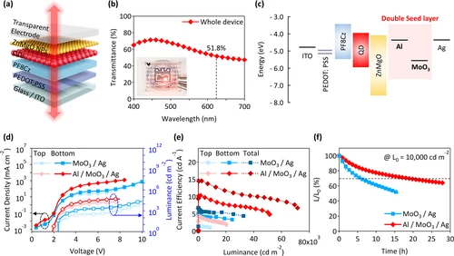
Transmittance of the device as a whole was 54.57% averaged over the visible range and 51.8% at 623 nanometres. That is about 9 points down from the 63.48% of the electrode alone, and it passes the 50% line usually taken as the baseline for transparent displays.
7. Does it work at two inches square
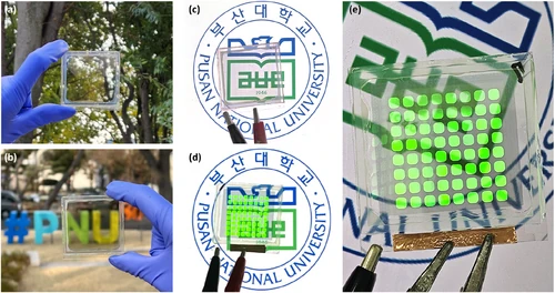
One laboratory pixel working and a screen working are different things. The team made an 8×8 pixel array on a 2-inch × 2-inch substrate. One pixel is 3 millimetres square.
Switched off, the background behind showed through both outdoors and indoors, and switched on, the whole array emitted evenly.
Why this demonstration matters connects back to the earlier reason for choosing thermal evaporation. Where solution-processed electrodes or graphene transfer lose uniformity over large areas, thermal evaporation is a process that covers a wide area evenly to begin with. Depositing two seed layers and one silver layer in turn does not lengthen the process sequence either.
8. What is left
The paper records two limitations of its own, and both point to the same place.
First, emission up and down is asymmetric. As the table showed, downward emission is more than twice the upward. Downward passes through ITO and upward through the silver electrode and the encapsulation glass, and the loss on the upper path is larger. For a device that puts double-sided emission forward, this asymmetry stays as a task, and the paper points to both raising the transparency of the upper electrode and reducing the optical loss of the encapsulation structure. An optical capping layer is the candidate.
Second, the absolute performance is not the best. The paper itself puts a comparison table against prior work and writes that “some prior studies have reported higher transmittance or efficiency.” The strength of this work is not a peak number but obtaining a low sheet resistance through simple sequential thermal evaporation, which suits large-area production.
One more thing is worth recording. These are results from a single red device. For a transparent display, the same electrode has to work in blue and green too, and when the wavelength changes the optical conditions of a thin metal film change with it. Seed layer thickness and silver thickness may have to be matched again for each colour.
Even so the place this work stands is clear. Transparent electrode research has long written performance in the two columns of transmittance and sheet resistance, while what actually held the device back was the third column. And admitting that three columns cannot be filled by one material, and dividing the layer, became the answer.
The remedy of splitting in two when one will not do is not itself new. What is new is confirming inside the device which axis had to be split. Because the electron-only devices and the work function measurement were put alongside a place where the electrode had only ever been measured as a film, that axis became visible.