
Surface treatment: AS (Anti-Static)
Today the anti-static layer sits not on the screen but on the protective film that gets peeled off and thrown away. Static is generated at the very surface that separates, so the anti-static layer moved from the base film to the adhesive face, and every reduction in static brought contamination and corrosion with it. The mainstream PEDOT:PSS is expensive but survived because it is used as thin as 0.03 micrometers, while CNT, which meets the same condition, still has to clear the wall of dispersion.
At the end of the moth-eye episode in Issue 7, we said the next episode would look at static electricity on the same cover window. This episode does cover that static, but one starting point changes.
Today the anti-static layer sits not on the screen but on the protective film that gets peeled off and thrown away. In public sources we found no evidence that current OLED cover surfaces carry an anti-static layer. Patents and specifications for process and shipping protective films, by contrast, are packed with anti-static figures.
The reason lies in where static is generated. As a panel moves through the process, protective films are attached and peeled off it many times. Static is generated at the very moment of peeling. This episode looks at where the layer meant to stop that moment has moved, what it paid for the move, and which materials are competing for that spot.
Static is generated the moment you peel
When two surfaces that were stuck together are pulled apart, they separate with one carrying a positive charge and the other a negative charge. This is called peel-off electrification. The faster the separation and the drier the air, the less chance the charge has to escape.
The size of the humidity effect is larger than you might expect. In an example compiled by ESDA, the electrostatic discharge industry association, walking across a carpet generates 35,000 volts at 10-25% relative humidity and 1,500 volts at 65-90%. That is why the international standard measures surface resistance on the dry side, at around 12% relative humidity.
| Range | Surface resistance | Meaning |
|---|---|---|
| Surface conductive | Below 10⁴Ω | Charge drains too fast and can spark |
| Surface dissipative | 10⁴-10¹¹Ω | Charge drains slowly; the range anti-static aims for |
| Surface insulative | 10¹¹Ω and above | Charge stays put |
The same association adds one more line. A low tendency to charge cannot be predicted from resistance alone. Generating less charge and draining the charge that has been generated are different jobs, and a protective film has to do both.
Cover surfaces are at a disadvantage here. There is a measured example of glass with an AF coating showing a surface resistance of 10¹³-10¹⁵Ω/□ (AGC patent). The smoother and more oil-repellent a surface is, the less path charge has to escape.
When reading kilovolt figures, look first at how they were measured. For the peel-off static in this episode, peel speed varies by company from 0.3 meters to 40 meters per minute, and the angle is a mix of 150 and 180 degrees.
The sensors differ too. Some read the surface potential every 10 milliseconds during peeling and take the maximum; others first apply 10 kilovolts to the sample before measuring. Change these conditions and the same film gives a different number, so figures from different companies must not be placed side by side and compared for size. Only comparisons within a single patent sit on the same scale.
In OLED, this charge can spread into mura on the screen. LG Display described in a patent how charge generated by friction between the cover window and outside objects seeps into the side of the panel, shifting the threshold voltage of the edge driver transistors, so that the edges turn brighter or take on a green tint.
The fix was not a surface coating but a ground path, such as conductive tape under and beside the panel and side coatings. Instead of blocking it on top of the screen, they drained it from the inside. So where is the anti-static layer left? On the protective film.
When do protective films go on and come off?
There is no public source summarizing how many times a single panel has protective films attached and peeled. Process-by-process cases, though, are scattered through the background sections of patents.
- Polarizer lamination: in methods that unroll the polarizer and attach it straight to the panel, lamination happens right where the carrier release film is peeled off. Nitto Denko wrote that the charged carrier induces charge on the panel, and ionizers cannot remove all of it
- Flexible OLED: static generated when the carrier substrate is detached changes TFT characteristics and creates mura. So Samsung Display attaches a lower protective film coated with 20-100 nanometers of PEDOT. Static is generated again when that film’s liner is peeled
- Encapsulation-layer protective film: the liner is peeled and the film attached, then once the process ends the film itself is peeled off again. That is twice. In an LG Chem patent, it was 2.5 kilovolts with the anti-static layer on one side only and 1.3-1.5 kilovolts with it on both sides
- After shipping: a Sharp LCD module specification states that “this module is sensitive to electrostatic discharge of 200 volts or more” and instructs keeping humidity at 50% or higher and using an ionizing blower when peeling the film
The separating surfaces are all different: carrier and panel, liner and adhesive, protective film and polarizer. This is where the question of which surface the anti-static layer should be on arises.
Why did the anti-static layer move to the separating surface?
Because static is generated at the separating surface, and it has to be drained at that surface. No matter how conductive you make the back of the film, if the adhesive face stays as it is, charge remains on the polarizer.
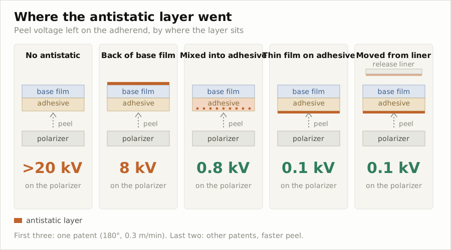
There are values measured under identical conditions. In a worked example from a domestic protective-film patent, this is the voltage left on a 17-inch polarizing film after the protective film was peeled at 180 degrees.
| Configuration | Voltage left on polarizing film |
|---|---|
| No anti-static | Over 20kV |
| Conductive polymer on both sides of base (1×10⁶Ω/□), ordinary adhesive | 8kV |
| Ionic anti-static agent in the adhesive | 0.8kV |
The 1×10⁶Ω/□ on the back of the base is conductive enough by the standard, yet 8 kilovolts remained. That conductive layer does not reach between the adhesive face, where the charge was generated, and the polarizing film.
So the industry kept moving the anti-static layer toward the separating surface. What had been coated on the base was mixed into the adhesive, and then laid on top of the adhesive face as a 0.1-0.3 micrometer thin film.
The final step is the release film. Fujimori Kogyo put the anti-static agent into the release layer of the release film and had it transfer onto the adhesive face when peeled. The surface resistance of the release face went from 5-6×10⁸Ω/□ before lamination to beyond the measurement range after peeling, while the adhesive face instead came to around 1×10¹⁰Ω/□.
Cutting static brings contamination with it
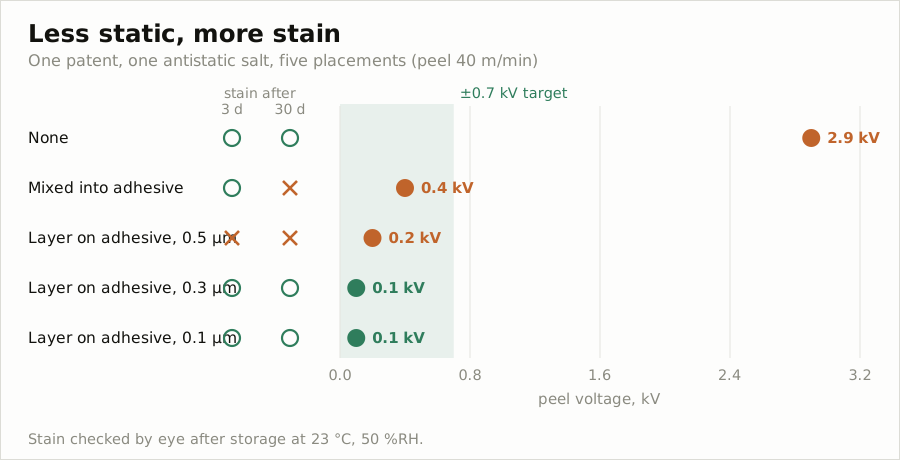
The closer the anti-static agent sits to the adhesive face, the lower the static, but the shorter the path for that substance to migrate onto the adherend. ZACROS (formerly Fujimori Kogyo) captured this trade-off in a single table by changing only where the same anti-static agent is placed.
Peel speed is 40 meters per minute, and the adherend is an AG polarizer.
| Placement | Peel-off static | Contamination after 3 days | Contamination after 30 days |
|---|---|---|---|
| None | 2.9kV | None | None |
| Mixed into adhesive | 0.4kV | None | Present |
| 0.5μm on adhesive face | 0.2kV | Present | Present |
| 0.1-0.3μm on adhesive face | 0.1kV | None | None |
Only the thinly applied layer controlled both static and contamination. Applied thickly, the voltage dropped further but contamination remained within three days. In the same document, ZACROS wrote that recent requirements are within plus or minus 0.7 kilovolts. As drive voltages have come down, so has the voltage that driver ICs and TFTs can withstand.
There is also a case showing that contamination is a heavier criterion than static. In one Nitto Denko protective-film patent, five comparative examples had peel-off static of minus 0.2 to 0 kilovolts, no different from the worked examples. But after 24 hours at 50 degrees and 92% humidity, all five failed the contamination evaluation. What decides the product is not the voltage figure.
That is why separate ways of measuring contamination developed. Nitto Denko deliberately laminates the film with bubbles, leaves it in high temperature and humidity, and looks at the marks left where the bubbles were. Adhesive components tend to migrate along the edges of bubbles.
There is also a numerical method. A test tape is applied to the glass the protective film was peeled from, its adhesion is measured, and that is divided by the value measured on clean glass. The lower this ratio, called the residual adhesion rate, the more something has been left on the glass. ZACROS also draws a ballpoint pen three times under a 500-gram load to see whether the mark transfers.
After contamination, the next price is metal corrosion. Patents describe lithium-salt anti-static agents, once widely added to adhesives, as damaging to metal. In 2012 Fujimori Kogyo used a pyridinium salt instead of lithium to avoid corroding aluminum foil, and later patents show a trend of dropping lithium or moving to halogen-free anions.
It was not only a lithium problem, though. In an LG Chem patent, a lithium-free quaternary ammonium salt also corroded copper and aluminum in a 1000-hour test, and in a Nitto Denko patent, copper under an adhesive with no anti-static agent at all lost 98% of its reflectance. Adding 0.1 part of a corrosion inhibitor cut that to 8%.
What changed was the victim. What the 2007-2012 patents set out to protect were the stainless steel and aluminum frames around LCD edges. Testing back then went no further than attaching aluminum foil and checking for discoloration.
From 2014-2015, metal-mesh copper and 500-nanometer aluminum and silver-alloy touch wiring appear. Sumitomo Chemical wrote that the pits formed under high temperature and humidity penetrate the metal layer. As the metal grew thinner, the same corrosion grew heavier, from a stain to an open circuit.
Six knobs that divide peel force into steps
After static, the next task is peel force. A process protective film has to come off easily when it needs to be peeled, and must not lift before then. The value differs by component. One example calls for 0.5-5gf/inch on a process protective film covering the polyimide substrate of a flexible panel (Samsung SDI patent). That is the force of peeling a 1-inch-wide film with a weight of a little over 5 grams.
The industry tunes this value by dividing it into steps like a staircase. There are six main knobs.
| Knob | What changes | Change in peel force | Price |
|---|---|---|---|
| Adhesive type | Silicone · urethane · acrylic | 0.04 · 0.14 · 0.23N/25mm under the same conditions | Silicone is expensive; urethane is hard to fine-tune |
| Formulation | Tackifier resin in silicone, 0→60 parts | 0.04 → 0.80N/25mm, 20 times | Too much resin causes re-peel failure |
| Formulation | Silicone slip agent in urethane, 0→15 parts | 6.8 → 1.4gf/25mm, about 5 times | Too much causes lifting after reliability tests |
| Peel speed | 0.3m → 30m per minute | Urethane 8-10 times, acrylic 16-60 times | Tune for low speed and high speed spikes |
| Switch | UV exposure or heating | UV 5 → 670gf/inch, heat several N → 0.3 or below | Adds an exposure or heating step |
| Interface hierarchy | Adhesion to base vs. to component | Base side 1.1 times or more | If reversed, the adhesive layer splits to both sides |
The adhesive type sets the order of magnitude, and the formulation tunes it by some multiple within that range. Shin-Etsu Chemical divides its silicone adhesives into four grades, from ultra-low tack at 0.02 up to high tack at 8.7N/25mm, and advises blending with the high-tack grade to get “any desired adhesion.” Silicone is not inherently ultra-low tack; it becomes ultra-low tack once the tackifier resin is taken out.
Peel speed makes it impossible to describe peel force with a single number. Because adhesive is a viscoelastic material, the faster it is peeled, the harder it resists. In an LG Chem patent, a film that measured 5.3gf/25mm at 0.3 meters per minute became 130gf/25mm at 30 meters. That is why the ratio of high speed to low speed itself is written into claims, as in “1-25.”
The switch type packs two steps into one film. Samsung SDI’s process film comes off easily at 5-29gf/inch before UV exposure, then rises to 580-840gf/inch after exposure and becomes a reinforcing film. Nitto Denko’s thermal-release sheets are graded on a grid that multiplies four release temperatures of 90, 120, 150 and 170 degrees by several steps of room-temperature adhesion, and drop to 0.3N/20mm or below when heated.
Interface hierarchy is the rule for processes that peel several layers in sequence. In a protective film for flexible use, Mitsubishi Chemical sets the force holding the adhesive layer to the base at 1.1 times or more, preferably 1.7 times or more, the force holding it to the component. If that is reversed, the adhesive layer splits into two faces and remains on the component. Double-sided release films likewise keep a 2-6 times difference between the heavy and light sides.
On the ultra-low-tack steps, the scariest thing is time. A comparative example in a Samsung SDI patent went from 30gf/inch to 220gf/inch in three days at 50 degrees. That is a 633% rise. Steps divided in units of a few gf can collapse several notches in three days, so companies also put “3-day increase of 10-80% or less” into their claims.
Where the anti-static layer squeezes in
At the bottom rung of the interface hierarchy, between the base and the adhesive layer. If the anti-static layer goes in there, the floor the adhesive layer holds onto becomes the anti-static layer instead of the base. If that floor is weak, the adhesive layer stays on the component the moment it is peeled.
So a PEDOT layer has a thickness window. In a Yulchon Chemical patent, 8 nanometers gave 6×10⁸Ω/□, not enough anti-static performance, and 1,100 nanometers had poor adhesion to the base. Both were satisfied at 100-200 nanometers. Nitto Denko wrote that beyond 300 nanometers the inside of the layer tears and cannot hold.
What guards that window is less the PEDOT itself than the binder used with it. In a Toray Advanced Materials patent, removing only the urethane binder from the same PEDOT coating dropped tape adhesion to the surface from 1,120 to 87g/in, to 1/13.
Mixing the anti-static agent into the adhesive shakes a different rung. Fujimori Kogyo wrote that this approach “makes fine adjustment of adhesion difficult” and that the amount migrating onto the adherend grows over time. Wherever the anti-static layer goes, it takes up one rung of the peel force staircase; that is the trade-off this episode is looking at.
Why is PEDOT:PSS mainstream despite being expensive?
Because it can be applied extremely thin. Supplier Nagase ChemteX writes that “PEDOT:PSS is expensive, but delivers the desired effect in a very small amount,” and gives the thickness needed for anti-static as about 0.03 micrometers.
PEDOT:PSS is a polythiophene-family conductive polymer. Because electrons flow along the polymer chain, unlike the ionic type, its resistance does not change with humidity. It can be coated as a water-based dispersion, and the same company’s comparison table rates its contamination of the adherend as “extremely low.” It meets almost every condition a protective film wants.
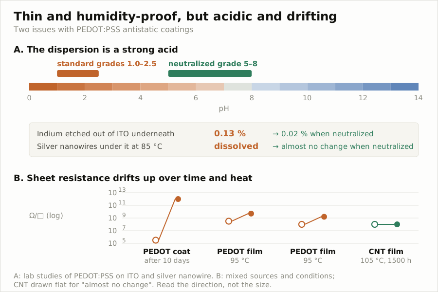
It has two weaknesses. One is acid. A PEDOT:PSS dispersion is a strong acid at pH 1.0-2.5 and leaches indium out of the ITO beneath it. There is also research showing it dissolves silver nanowires at 85 degrees. This is why suppliers release acidic and neutral grades separately.
The other is that resistance rises with time and heat. A Dongjin Semichem patent wrote that conventional coatings rose from 10⁵-10⁶Ω/□ to 10¹²Ω/□ after ten days. Nitto Denko wrote that over time PSS detaches from PEDOT, raising surface resistance and peel-off static, followed by oxidation and photothermal degradation.
Placed side by side, the three routes look like this.
| Ionic (mixed into adhesive) | PEDOT:PSS (coating) | CNT (coating) | |
|---|---|---|---|
| Charge carrier | Ions | Electrons along polymer chains | Electrons in nanotubes |
| Humidity | Many types weaken when dry | Unaffected | Unaffected |
| Thickness or amount needed | A few parts added | About 0.03μm | Content around 0.1-0.3% |
| Weakness | Bleed-out and contamination, metal corrosion | Strong acid (pH 1-2.5), resistance rise from PSS detachment | Dispersion, residual dispersant |
| Heat and moisture | Cases of resistance spiking after high temperature | Resistance rises at 95℃ | Almost no change at 105℃ for 1500 hours |
What does CNT have to overcome?
Dispersion. CNT meets the same condition as PEDOT, being used thin in a very small amount, and is tougher against heat and moisture. The remaining wall is untangling the strands one by one and spreading them evenly.
Start with the evidence that it meets the condition. Nagase ChemteX’s comparison table rates material cost in the same grade for both PEDOT and CNT, and rates CNT higher for durability. This is a table from a company that sells PEDOT.
LG Display and Nano Solution filed a patent replacing a PEDOT:PSS anti-static film with single-walled CNT. As the reason, they cited the drop in reliability of PEDOT films under high temperature and humidity. While the sheet resistance of the PEDOT film kept rising at 95 degrees, the CNT film held almost unchanged for 1500 hours at 105 degrees.
This film is not a protective film but a layer that goes permanently inside the panel. Still, by reaching 98.5-100% transmittance with a CNT content of 0.13-0.26%, it shows that CNT also meets the condition of being used thin.
There is also one result that matters for protective-film processes. In a Nan Ya Plastics patent on protective tape for semiconductor wafers, corona-treating the surface collapsed a conductive-polymer anti-static layer from 10⁷·⁸ to 10¹⁴·⁵Ω/sq. After the same treatment, a CNT layer actually dropped slightly, from 10⁷·⁸ to 10⁷·⁵. It is not for displays, but the direction is clear.
There are conditions on the material side too. Multi-walled CNT costs less than 1 dollar per gram, but single-walled CNT costs several hundred dollars per gram. The same review notes that about 1/3 of a CNT film is metallic and 2/3 semiconducting, so a barrier forms wherever the two meet, increasing resistance.
Now the wall. CNTs are long relative to their diameter and have a large surface area, so they stick to one another through van der Waals forces. They form bundles that tangle again into clumps. Toray wrote in a patent that this bundle structure is “the biggest obstacle to industrial use of CNT.”
Untangling bundles requires putting in energy, but too much breaks the CNTs. In Toray’s worked examples, at a reference transmittance of 87%, a well-dispersed film was 550Ω/□. Both an under-dispersed film and a film whose CNTs had been shortened to 1.8 micrometers by excessive ultrasonication came out at 680Ω/□. Too little or too much, both are a loss.
The dispersant that helps dispersion is a necessary evil. Left in the film, it is an insulator and raises the contact resistance between CNTs. Washing it out with acid lowers resistance but oxidizes the CNT surface. In one study, increasing nitric-acid treatment brought sheet resistance down to 132Ω/sq, but transmittance fell below 80% and the defect index rose from 0.30 to 0.41.
A single dispersant can flip the outcome. In the LG Display and Nano Solution patent above, a film dispersed with polyacrylic acid was 10⁸Ω/□, but switching to a surfactant turned dispersibility, stability, coatability and transmittance all to poor, and sheet resistance rose to 10⁹·⁴Ω/□.
A review of transparent conductive films sums it up this way: “The lack of a feasible dispersion technology severely hinders the industrial use of wet-processed CNT films.” And it adds: the CNT transparent films that reached mass production, from Foxconn and Canatu, both used dry processes that need no dispersion.
In the simulator below you can see for yourself why dispersion is a wall. The same amount of CNT is scattered on a film, and the only thing that changes is whether incomplete dispersion leaves several strands tangled into clumps. Whether a path forms between the electrodes at both ends is actually computed every time.
Switch from Well dispersed to Aggregated and the same CNTs gather into clumps of ten strands each. Inside a clump it is dense, but the space between clumps is empty and the connection breaks. Out of 20 random layouts, not a single one connects.
To reconnect it, CNT amount has to go up to around 4, twice the starting value. It absorbs that much more light. Enlarge the clump radius, that is, make them clump less, and even the same amount starts to connect again.
Near the threshold, for example with CNT amount at 1.0 in the dispersed state, each press of New random layout sometimes connects and sometimes breaks. Near the threshold, even the same formulation gives split results, and this is why a film whose useful tubes have been reduced by aggregation gets pushed toward that threshold and becomes unstable.
To sum up: the anti-static layer moved to the surface where static is generated, the separating surface. The more static was reduced, the more contamination and corrosion followed, and PEDOT:PSS, used thin, remained the mainstream. CNT, which meets the same condition, stands before the process wall of dispersion.
The next episode looks at the bottom layer all of these layers rest on, the hard coat (HC).